Chapter/Index: Introduction | A | B | C | D | E | F | G | H | I | J | K | L | M | N | O | P | Q | R | S | T | U | V | W | X | Y | Z | Appendix
| The Nsense and Psense amplifiers (NSA and PSA) in DRAM, as shown in Figure 4207a, are carefully designed to work together to: Critical consideration of the design of sense amplifiers are:
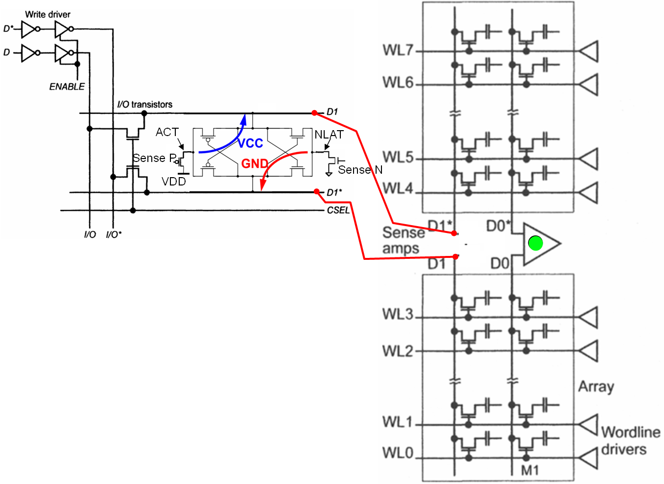
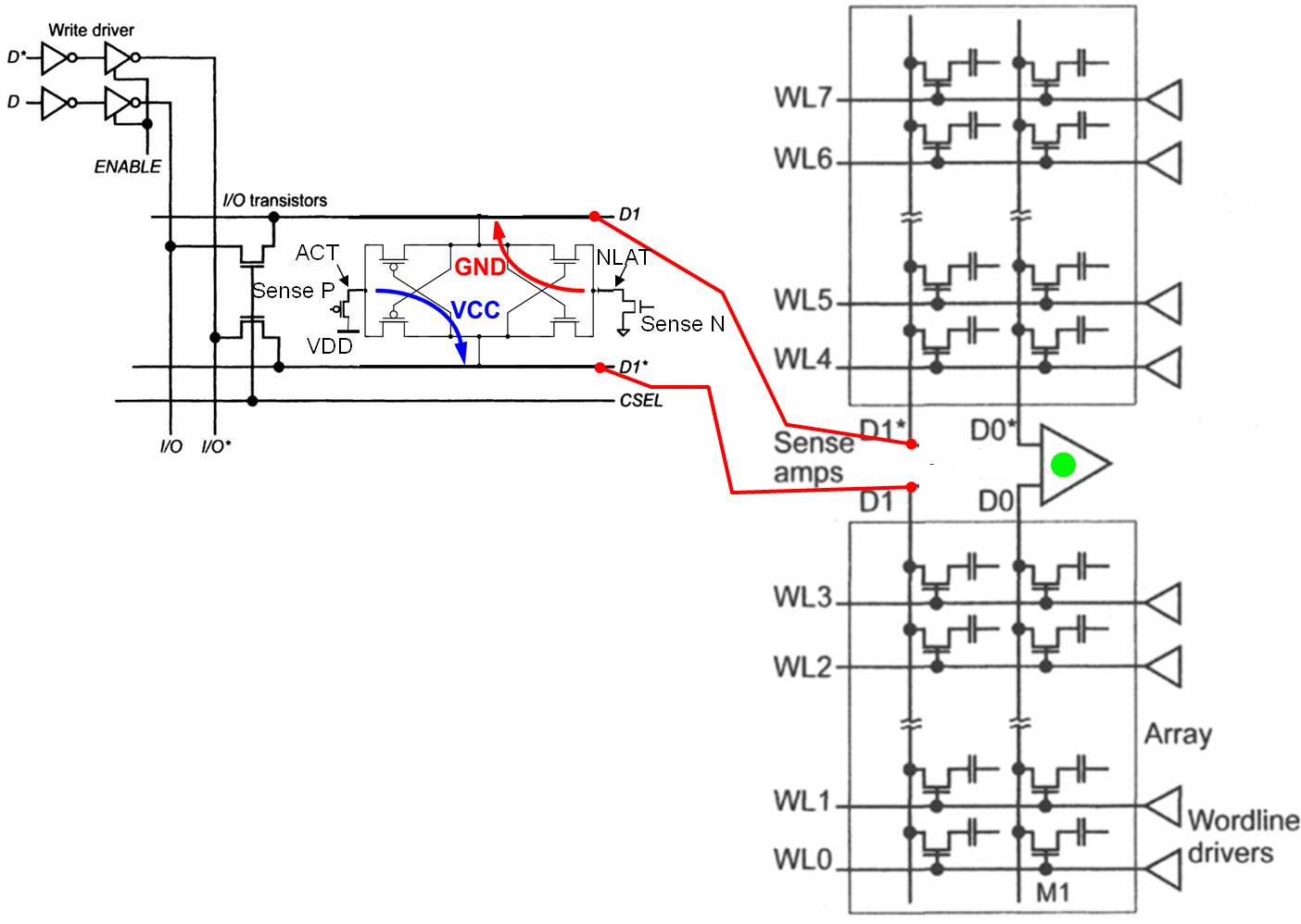
Figure 4207b shows sense amplifier schematic with I/O devices, indicating that: Initially, ACT is at VSS (GND) and NLAT* held at VCC/2. while both D1 (BL1) and D1* (BL1*) are at VCC/2 as well. The start of the read operation is the node sense N, which have 0V voltage levels. When reading, the wordline is pulled to VCC+Vth and BL1/* changes. After the cell has been accessed, a sense amplifier pulls up the voltage differential between the two column lines. The sensing is essentially the amplification of the differential voltage between the two column lines D1 and D1*. The P sense amplifier and the N sense amplifier are normally fired sequentially. The NSA is first fired by bringing NLAT* (N sense-amplifier latch) toward ground. The voltage difference between NLAT and the column lines increases so that the NMOS transistor whose gate is connected to the higher voltage column line begins to conduct. Such conduction causes the low-voltage column to be brought to discharge towards NLAT* and finally to be brought to ground voltage. However, the other NMOS transistor will not conduct. In some cases, after the N sense amplifier has fired, ACT (for active pull-up) will be brought towards VCC to activate the P snese amplifiers. The low-voltage column line is close to ground so that the corresponding PMOS transistor is driven into conduction. This charges the high-voltage column line towards ACT and ultimately towards VCC. Therefore, all column lines are either driven to high or to low according to the contents of the DRAM cell in the row.
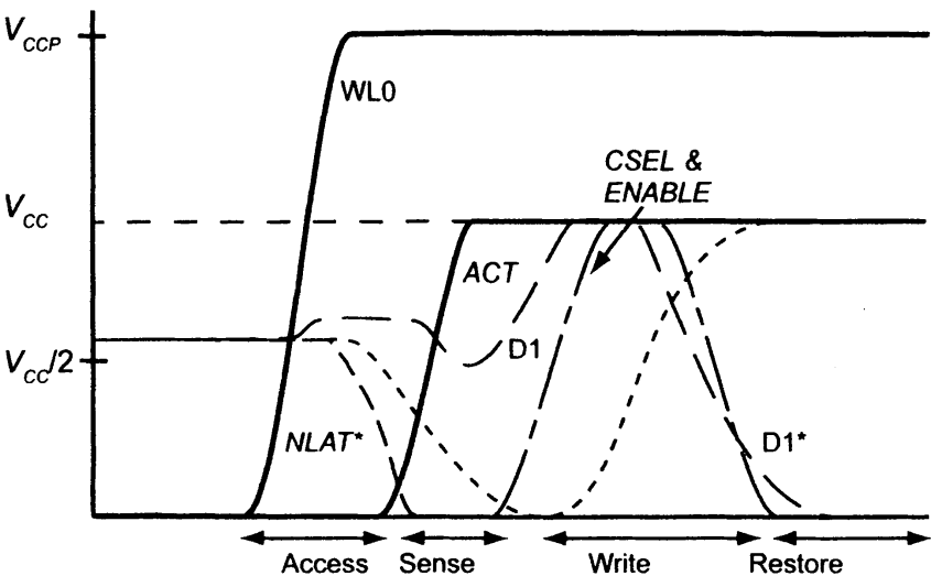
The Write driver simply overdrives the sense amplifiers. Figure 4207c shows the Write operation waveforms in DRAM.
[1] Brent Keeth, R. Jacob Baker, Brian Johnson, Feng Lin, DRAM Circuit Design: Fundamental and High-Speed Topics , 2nd Edition, 2007.
|