Integrated Circuits and Materials

An Online Book, First Edition by Dr. Yougui Liao (2018)

Practical Electron Microscopy and Database - An Online Book

Chapter/Index: Introduction | A | B | C | D | E | F | G | H | I | J | K | L | M | N | O | P | Q | R | S | T | U | V | W | X | Y | Z | Appendix

Bias Conditions for (Leakage) Current Measurements

Different voltage conditions at the source/drain, and the bulk result in different intrinsic leakage paths. The different leakage current contributions to the total off leakage depend on the bias for the MOSFET.

Table 4742a. Bias conditions for leakage current measurements.

Purpose Leakage state Measurement & stress Vg (gate) Vd (drain) Vs (source) Vb (sub) Application Reference
    SILC measurement 0 ~ -6 V Floating Floating 0 V   [1]
    Junction leakage 0 V 0 V Floating 0 ~ -3 V   [1]
    GIDL measurement 0 V 0 ~ 6 V Floating -0.8 V   [1]
    F-N stress (10 s) -7 V Floating Floating 0 V   [1]
    GIDL stress (10 s) 0 V 7 V Floating 0 V   [1]
Compa Off-current leakage IDrainc 0 V 0 ~ 2V 0 V 0 V Peripheral DRAM transistor [2]
Off-current leakage IDrain = ISource d 0 V 0 ~ 2V 0 ~ 2V

0 V

Peripheral DRAM transistor [2]
a. Comp: Comparison.

Schematic drawing of the cell transistor for biasing

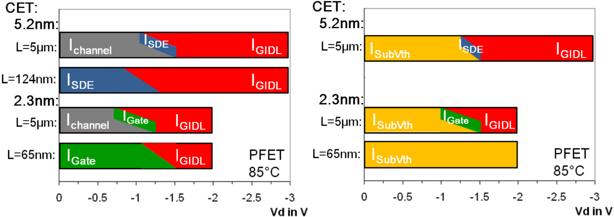
Figure 4742a. Schematics of the cell transistor for biasing. [1]

Figure 4742b shows the measured leakage currents. The subthreshold-, gate overlap-, channel- and gate induced drain leakage current are the main contributions to the total peripheral transistor off-current.

Schematic of the measured leakage currents
(a)
(b)
Figure 4742b. Schematic of the leakage currents: (a) Measured with the condition "d" in Table 4742a, and (b) Measured with the condition "c" in Table 4742a. [2]

Figure 4742c shows that the dominant leakage current mechanisms of the total leakage depending on the bias.

Schematic of the measured leakage currents
(a)
(b)
Figure 4742c. The bar graph shows the main leakage current contribution to the total off-current for short: (a) With the condition "d" in Table 4742a, and (b) With the condition "c" in Table 4742a. [2]


[1] Kwan-Yong Lim, Se-Aug Jang, Yong Soo Kim, Heung-Jae Cho, Jae-Geun Oh, Su-Ock Chung, Sung-loon Lee, Woo-Kyung Sun, Jai-Bum Suh, Hong-Seon Yang, and Hyun-Chul Sohn, Impact of gate sidewall spacer structures on DRAM cell transistors under Fowler-Nordheim and gate-induced drain leakage stress conditions, 2004 IEEE International Reliability Physics Symposium. Proceedings, DOI: 10.1109/RELPHY.2004.1315376, 2004.
[2] Leakage Current and Defect Characterization of Short Channel MOSFETs, DOKTOR-INGENIEUR, vorgelegt von, Guntrade Roll, Erlangen, 2012.