| Extreme ultraviolet (EUV) lithography is a soft X-ray technology with a wavelength of 13.5 nm. EUV presents numerous challenges, chief among them being its tendency to be absorbed by nearly all materials, including air and lenses. As a result, an EUV scanner (also known as a stepper) must operate in a complete vacuum, and its optics must rely on reflective surfaces (mirrors) rather than refractive ones (lenses). EUV scanners enable resolutions down to 22 nm half-pitch. An EUV light source makes use of a high power laser to create a plasma. EUV was considered a critical component at 16/14 nm nodes as a way of avoiding double patterning using 193 nm immersion. At 7 nm, single patterning is possible with EUV, but is a relatively slow operation with current resists and can cause unwanted random defects in patterns. At 5 nm, double patterning will be required on the critical layers even with EUV. Even though it requires more expensive steps, double patterning means the pitches of features can be relaxed and then processed, which can reduce the number of defects.
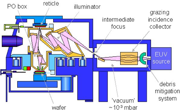
Figure 4849a. EUV lithography. [4]
In the semiconductor industry and in leading research laboratories, EUV patterning technologies have been studied for advanced processes and applications such as development of 20 nm period line/space patterns. [1]
The printed feature of EUV is shifted and biased on the wafer due to
oblique illumination of the mask. Consequently, target CD and pattern position are changed in accordance with pattern
direction, pattern type and slit position of target pattern. [2]
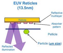
Figure 4849b. EUV reticles. [4]
The main properties of EUV are:
i) Can be easily absorbed by any kind of matters. Even a small amount of air can be a formidable barrier to its transmission. As a result, the entire lithography must take place in the high vacuum, which was never the case before.
ii) Reflective mirrors need to be used. Refractive lenses cannot be used because EUV is strongly absorbed by any materials. Furthermore, there’s no good EUV reflector either. Even the multilayered Bragg reflector absorbs around 30% of EUV lights.
iii) EUV beam needs to be shaped by a dozen such mirrors. By the time the EUV beam hits the wafer, the beam is attenuated by 99%.
iv) If the power received is too low, it will require a longer exposure, which will severely limit the throughput.
v) Producing the EUV beam is a challenging task. When the EUV program was initiated there were no suitable EUV light sources on the market.
vi) The light source creates debris, the EUV light degrades the mirror surfaces and creates debris.
vii) EUV is way more sensitive to debris size because the wavelength is so small.
viii) EUV produces random defects with no obvious solution below 7 nm, reported in EETimes, although it works acceptably for 7 nm or larger processes. These problems include both areas where material is not fully etched away, causing shorts between lines in the chip, and areas where too much is etched away, causing gaps and tears where the material should be continuous. Research is needed to improve the photoresists, to understand their behavior when exposed to EUV and to reduce the number of defects. If these problems cannot be ironed out, they may force a different approach to chip design.
ix) With EUV, we can draw clearer circuit on a wafer than using ArF. Better pattern fidelity brings higher design flexibility and better performance.
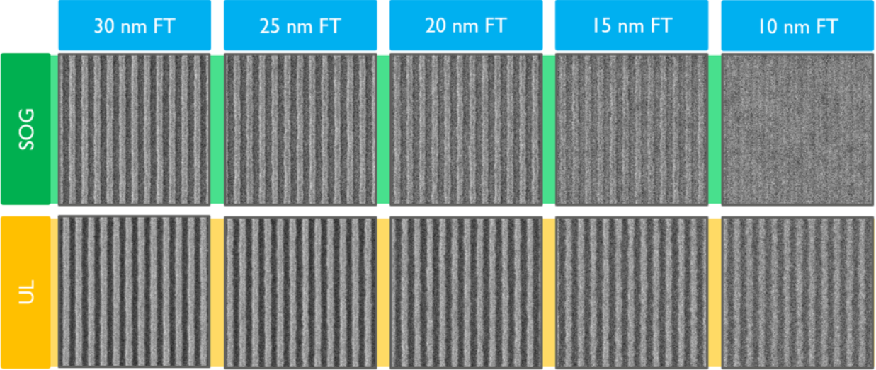
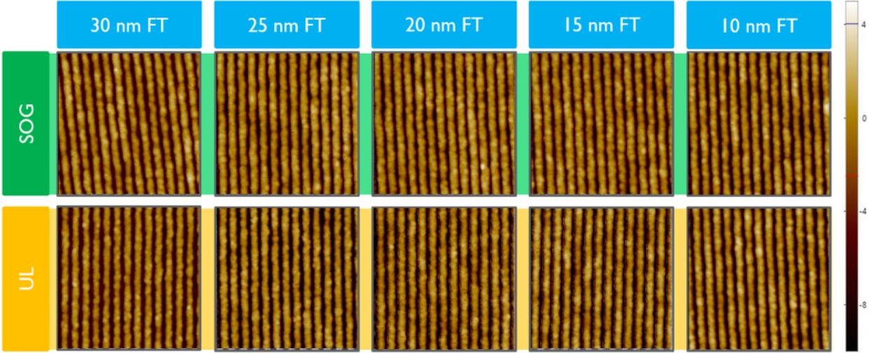
It is expected that, for high NA EUVL, the challenges can be subdivided into: [8]
i) Metrology challenges due to reduced CDSEM image quality. The design of experiments for the metrology can be used to address this challenge:
i.a) Visual comparison of the CDSEM images of the various resist film thicknesses (FTs).
i.b) Verification of the resist array height compared to
the nominal resist FT by AFM (see Figure 4849c).
i.c) Assessment of the quality of the CDSEM images with the
signal-to-noise ratio (SNR).
i.d) Determination of the CD 3σ precision of a full CDSEM
image.
i.e) Simulation can be used to further strengthen the experimental data.
ii) Challenges related to resist patterning performance. These challenges can be addressed through:
ii.a) Determination of the uLWR scaling
through resist FT.
ii.b) A CDSEM frame variation study to further elucidate that observed uLWR scaling.
ii.c) Simulation can be used to further strengthen the experimental data.
| Figure 4849c. Measurements of resist FT variation (30, 25, 20, 15, and 10 nm) on an SOG UL: (a) CDSEM images, and (b) AFM images. [8] |
Atomic absorption cross sections σa of EUV light source with atomic number Z from 1 to 86 are shown in Figure 4849d.
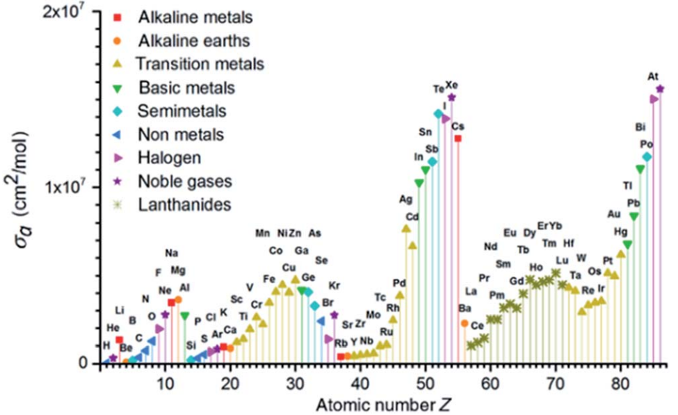
| Figure 4849d. Atomic absorption cross sections σa of EUV light source with atomic number Z from 1 to 86. [6] |
Cost of ownership (COO) is the analysis of all costs associated with the acquisition, use and maintenance of a good or service. Figure 4849e shows COO of EUV
lithography. EUV technology is cost effective process if throughput of EUVL is improved over 100 wph.
[3]
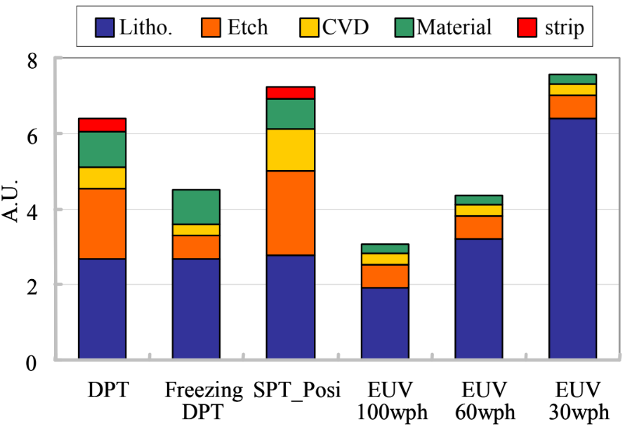
Figure 4849e. COO of EUV
lithography.
[3]
Table 4849. EUV masks.
| Mask name |
Absorber |
Capping layer |
Defects on mask |
Reference |
| LTEM |
TaN |
Si |
Slight footing profile |
[3] |

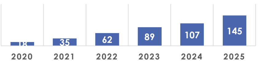
Figure 4849f. Prediction of EUV sales. [5]
| Figure 4849g. (a)
EUV photoresist revenues
(US$ millions) and (b)
EUV photoresist volumes
(kiloliters). [7] |
Single-expose (SE) extreme ultraviolet (EUV) lithography suffers from random variations caused by local fluctuations in
i) Shot noise.
ii) Chemical reactions.
With the scaling to extend SE EUV to smaller pitches, these variations result in postdevelop defects, such as resist line bridges or breaks, which impact electrical yield and narrow the size of the process window (PW) as defined by critical dimension (CD). [9] Characterization of random defects postdevelop provides early PW centering which correlates to electrical yield parameters, limiting the number of defects that enter downstream processes. Defect-free PW characterization allows for co-optimization of patterning processes and materials; however, this cannot be accomplished with-out a stable test vehicle and robust characterization methodology. [10]
[1] Kanghyun Kim, Jong-Won Lee, Byeong-Gyu Park, Hyun-Taek Oh, Yejin Ku, Jin-Kyun Lee, Geunbae Lim and Sangsul Lee, Investigation of correlative parameters to evaluate EUV lithographic performance of PMMA, RSC Advances, 2022, 12, 2589.
[2] T. Schmoeller et. al., EUV pattern shift compensation strategies, Proc. SPIE 6921, (2008).
[3] Tae-Seung Eom, Sarohan Park, Jun-Taek Park, Chang-Moon Lim, Sunyoung Koo, Yoon-Suk Hyun, HyeongSoo Kim, Byung-Ho Nam, Chang-Reol Kim, Seung-Chan Moon, Noh-Jung Kwak, Sungki Park, Comparative study of DRAM cell patterning between ArF immersion and EUV lithography, https://doi.org/10.1117/12.814378, SPIE Advanced Lithography, 2009.
[4] www.quora.com.
[5] Visible Alpha 2019.
[6] Chaoyun Luo, Chanchan Xu, Le Lv, Hai Li, Xiaoxi Huang and Wei Liu, Review of recent advances in inorganic
photoresists, RSC Adv., 10, 8385, (2020).
[7] Warren Montgomery, 2021 Techcet’s Critical Materials Reporttm Lithography Materials Photoresists, Extensions & Ancillaries, 2021.
[8] Joren Severi, Gian F. Lorusso, Danilo De Simone, Alain Moussa, Mohamed Saib, Rutger Duflou and Stefan De Gendt, Chemically amplified resist CDSEM metrology exploration for high NA EUV lithography, Journal of Micro/Nanopatterning, Materials, and Metrology, 21(2), 021207, https://doi.org/10.1117/1.JMM.21.2.021207, (April 2022).
[9] P. De Bisschop and E. Hendrickx, “Stochastic printing failures in EUV lithography,” Proc.
SPIE 10957, 109570E (2019).
[10] L. Meli et al., “Defect detection strategies and process partitioning for single-expose EUV
patterning,” J. Micro/Nanolithogr. MEMS MOEMS 18(1), 011006 (2018).
|