In theory, for FinFETs, the OFF-current, leakage current, GIDL, and subthreshold swing increase with increasing temperature, whereas the ON-current, low-field mobility, and threshold voltage decrease with temperature. [5]
Figure 4895a shows a FinFET structure with critical dimensions.

Figure 4895a. FinFET structure with critical dimensions. [6]
Figure 4895b shows transistor fin improvements from generations to generations.

Figure 4895b. Transistor fin improvements from generations to generations. [6] |
Figure 4895c shows the schematic diagram of Junctionless Accumulation-Mode (JAM) bulk FinFET structure for n-channel operation.
| Figure 4895c. Schematic diagram of Junctionless Accumulation-Mode (JAM) bulk FinFET structure, for n-channel operation, Two fin top widths. [1] |
| As complimentary techniques, both atom probe tomography (APT) and secondary ion mass spectrometry (SIMS) had been used to study fin sidewall doping by plasma implantation (PLAD). For instance, Figure 4895d shows TEM cross-section of fin, APT reconstruction, and corresponding
mass-spectrum. The APT reconstruction image presents dopants in
both the sidewall and fin top. |
| Figure 4895d. (a) TEM cross-section of fin, (b) APT reconstruction, and (c) corresponding
mass-spectrum. [2] |
| 1.5-D SIMS had been used to extract the sidewall dopant concentration, as shown in Figure 4895e, which was demonstrated as a reliable process monitor allowing measurement of total implant dose into the sidewall and doping conformality around the fin. [3] |
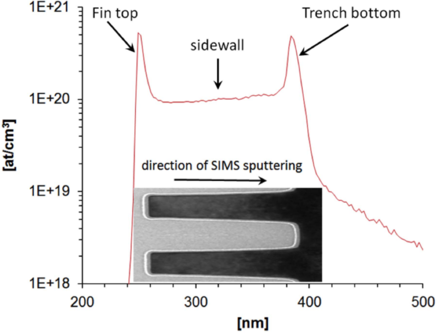
Figure 4895e. SIMS analysis result of As in the Fin structure. [2] |
Figure 4895f shows the 3D structures of CMOS, FinFET, Nanosheet and 3D VTFET.
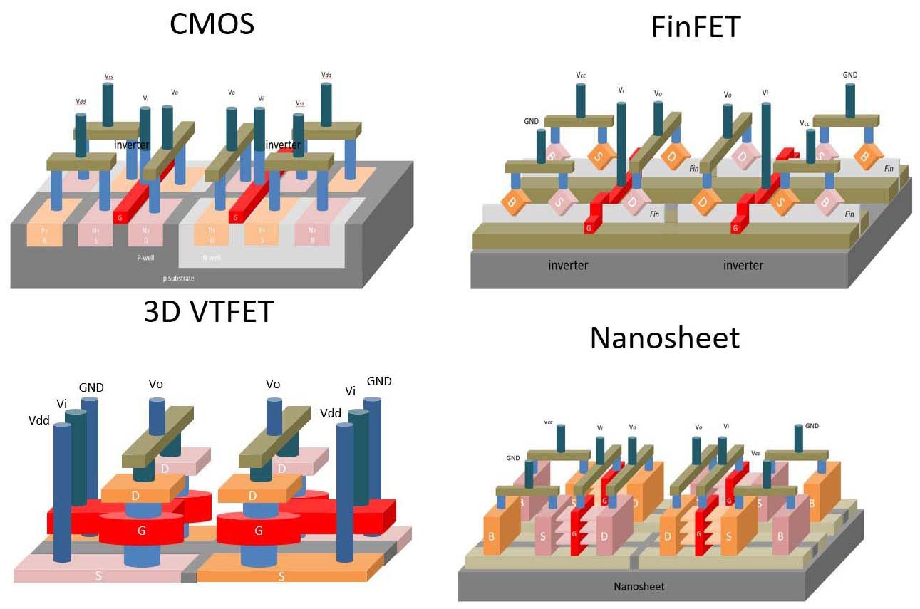
Figure 4895f. 3D structures of CMOS, FinFET, 3D VTFET and Nanosheet. [4] |
[1] Kalyan Biswas, Angsuman Sarkar, Chandan Kumar Sarkar, Fin shape influence on analog and RF performance of junctionless accumulation-mode bulk FinFETs, Microsystem Technologies, DOI: doi.org/10.1007/s00542-018-3729-1, (2018).
[2] Dimitry Kouzminov, James Cournoyer, Somchintana Norasetthekul, Harish Muthuraman and Qi Gao, Quantitative Aspects of PLAD Sidewall Doping Characterization by SIMS and APT, Microscopy and Microanalysis, doi:10.1017/S1431927618015301, (2018).
[3] Vandervorst W, Fleischmann C, Bogdanowicz J, Franquet A, Celano U,
Paredis K and Budrevich A, Dopant composition and carrier
profiling for 3D structures. Mater Sci Semicond Process 62, 31–48, (2017).
[4] Woong Jae Chung, https://media.licdn.com/dms/image/C4E22AQG9yGZmntcisQ/feedshare-shrink_800/0/1676746914271?e=1679529600&v=beta&t=OgtrMY48-L0WAF5eHSTQE8vGkzuO94m8YD-u-GNYmLk, (2023).
[5] Amer Diab, Galo A. Torres Sevilla, Sorin Cristoloveanu, and Muhammad Mustafa Hussain, Room to High Temperature Measurements of Flexible SOI FinFETs With Sub-20-nm Fins, IEEE TRANSACTIONS ON ELECTRON DEVICES, VOL. 61, NO. 12, DECEMBER 2014.
[6] https://www.anandtech.com/show/13405/intel-10nm-cannon-lake-and-core-i3-8121u-deep-dive-review/3.
|


