tRCD is Row to Column command Delay in ns (also called ACTIVATE to internal READ or WRITE delay), which is the time interval between row access and data ready at sense amplifiers (SA), which is the time that the data arrives at SA after the row is turned on. Figure 4956a shows the data transfer from CPU to DRAM memory in a computer.

| Figure 4956a. Data transfer from CPU to DRAM memory in a computer. tRCD is indicated by the black arrow. [6] |
Figure 4956b
shows that before a row-access operation, the bitline
is precharged, and the voltage on the bitline is set to
the reference voltage, Vref, as well as illustrates the relationship between
two important timing parameters: tRCD and tRAS. In phase one, the wordline
voltage is overdriven to at least Vt above Vcc, and the
DRAM cell discharges the content of the cell onto the bitline and raises the voltage from Vref to
Vref+. In
phase two, the sense control signals SAN and SAP are
activated in quick succession and drive the voltage
on the bitline to the full voltage. Then, the voltage on the
bitline restores the charge in the DRAM cells in
phase three.
Although the relative durations of tRCD and tRAS are not drawn to scale, after
time tRCD, the sensing operation is complete, and
the data can be read out through the DRAM device’s
data I/O. However, after a time period of tRCD from
the beginning of the activation process, data is yet to be restored to the DRAM cells. The data restore operation is completed after a time
period of tRAS from the beginning of the activation
process, and the DRAM device is then ready to accept
a precharge command that will complete the entire
row cycle process after a time period of tRP.
Here, the term definitions are:
Bitline
CSL
Vref
tRCD
tRAS
VCC
tRP
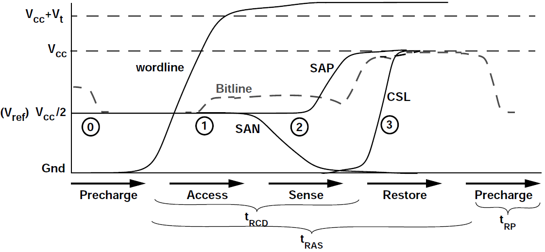
Figure 4956b. Simplified sense amplifier voltage waveform. Read(1) as an example. [1] |
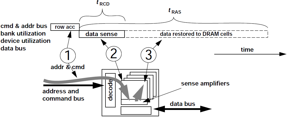
Figure 4956c. Row access command and timing. [1]

Figure 4956d. Posted CAS defers CAS commands in DRAM devices by a preset delay value, tAL. [1]
| Figure 4956e. Consecutive column-read commands to different rows of the same bank: best-case scenario. [1] |
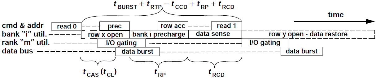
As shown in Figure 4956f, the read access in DRAM starts with an ACT (ACTIVATE)
command to bring the required row into the sense amplifiers, and then a RD (READ) command
is issued to fetch data from this row buffer. The interval between ACT and RD is constrained
by tRCD. DRAM read is destructive, and thus the charge in the storage capacitors needs to
be restored. The restore operation is performed concurrently with RD, and a row cannot be
closed until restoring is done, which is determined by tRAS-tRCD. Once the row is closed,
a PRE (PRECHARGE) can be issued to prepare for a new row access. PRE is constrained
by timing tRP. The time for the whole read process is tRC=tRAS+tRP. [4]

Figure 4956f. Commands and timing constraints involved in DRAM accesses. [3] |
Figure 4956g shows the Row Active Command.
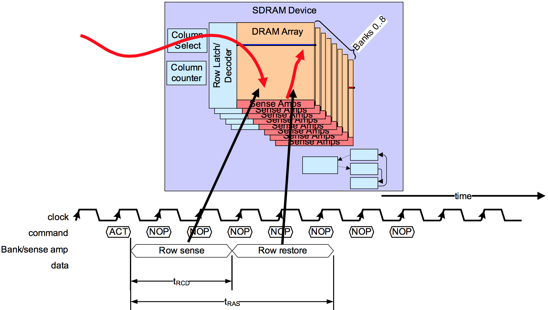
Figure 4956g. Row Active Command. [5] |
Table 4956. External DRAM controller parameters on DRAM board. [2]
| Parameter |
Description (unit) |
| Write buffer size |
Number of write queue entries |
| Read buffer size |
Number of read queue entries |
| Write high/low threshold |
High/low watermark for write queue |
| Scheduling policy |
FCFS or FR-FCFS |
| Address mapping |
RoRaBaCoCh, RoRaBaChCo, RoCoRaBaCh [3] |
| Page policy |
Open or closed (adaptive or not) |
| Frontend latency |
Static frontend latency (ns) |
| Backend latency |
Static backend latency (ns) |
| Device bus width |
Data bus with per DRAM device (bits) |
| Burst length |
DRAM burst length (beats) |
| Row-buffer size |
Device row buffer size (bytes) |
| Devices per rank - |
|
| Ranks per channel - |
|
| Banks per rank - |
|
| Channels |
Channel count for the address decoding |
| tRCD |
Row to column delay (ns) |
| tRAS |
Row access strobe (ns) |
| tRP |
Row precharge time (ns) |
| tCL |
Column access latency (ns) |
| tBURST |
Burst duration (ns) |
| tRFC |
Refresh cycle time (ns) |
| tREFI |
Refresh command interval (ns) |
| tWTR |
Write to read switching time (ns) |
| tRRD |
Row to row activation delay (ns) |
| tXAW |
Activation window (ns) |
| Activation limit |
Number of activates in window |
[1] Bruce Jacob, Spencer W. Ng, and David T. Wang, Memory Systems: Cache, DRAM, Disk, 2008.
[2] Andreas Hansson; Neha Agarwal; Aasheesh Kolli; Thomas Wenisch; Aniruddha N. Udipi, Simulating DRAM controllers for future system architecture exploration, 2014 IEEE International Symposium on Performance Analysis of Systems and Software (ISPASS), DOI: 10.1109/ISPASS.2014.6844484, (2014).
[3] JEDEC, . DDR3 SDRAM specification, 2009b.
[4] Xianwei Zhang, Exploration of DRAM Scaling From Restoring Perspective, Thesis, 2016.
[5] http://www.wowotech.net/basic_tech/.
[6] www.cnblogs.com/.
|