Chapter/Index: Introduction | A | B | C | D | E | F | G | H | I | J | K | L | M | N | O | P | Q | R | S | T | U | V | W | X | Y | Z | Appendix
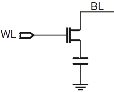
| The DRAM array employs a one-transistor and one-capacitor (1T1C) as a memory cell, where the capacitor stores a charge as a data bit. The charge in the capacitor is read or written through the access transistor when it is switched. The capacitor maintains the data bit (i.e. 1 for VDD, and 0 for 0 V) when the access transistor is off. The read process of all memory devices is common. After settling the predefined voltage to the bit line, the bit line is electrically connected with the memory cell. Then, the stored bit information of the cell will modulate the bit line voltage or current. The modulated analog value (voltage or current) of a bit line is then converted to the digital value (namely, GND or VDD) by the sense amplifier (SA) circuit.
Figure 4997a. DRAM and its equivalent circuit models. [1] In charging a load capacitor C up ΔV volts and discharging it to its original voltage, a gate pulls an amount of current equal to C·ΔV from the VDD supply to charge up the capacitor and then sinks this charge to ground discharging the node. At the end of a charge/discharge cycle, the gate/capacitor combination has moved C·ΔV of charge from VDD to ground, which uses an amount of energy equal to C·ΔV·VDD that is independent of the cycle time. The primary
focuses for traditional DRAM development: The primary
focuses for embedded DRAM development: Cell replacement and error correction codes
are currently adequate to address yield and reliability problems facing DRAM manufacturers.
[1] Krzysztof (Kris) Iniewski, CMOS Processors and Memories, 2010.
|