Chapter/Index: Introduction | A | B | C | D | E | F | G | H | I | J | K | L | M | N | O | P | Q | R | S | T | U | V | W | X | Y | Z | Appendix
| The MOS transistor (MOS for Metal Oxide Semiconductor) is by far the most important basic element of an integrated circuit. When
it is on, it allows current to flow, and when it is off, it stops current from flowing. Such MOS switch is
turned on and off by electricity. Two types of MOS devices exist in CMOS technology (Complementary
Metal Oxide Semiconductor):
Figure 4999a. NMOS and PMOS. The p-channel MOS is built by using polysilicon as the gate material and P+ diffusion for the source and drain. The pMOS device requires the addition of the n-well layer to the polysilicon and diffusion layers. The P+ diffusion must be completely included inside the n-well layer, in order to work properly. Figure 4999b shows PMOS and NMOS diagrams.
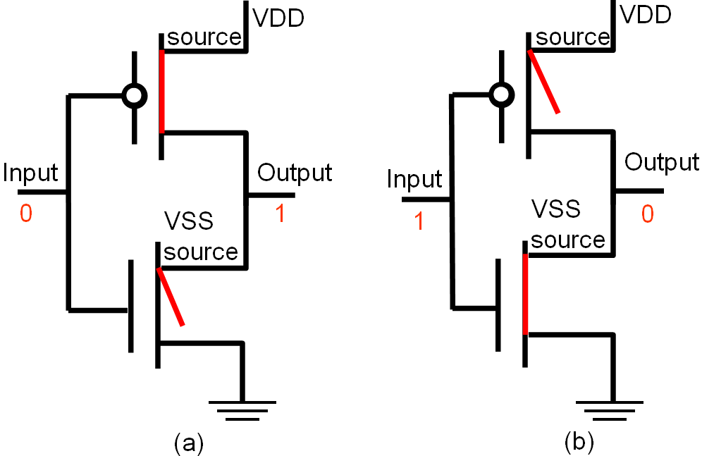
Figure 4999b. PMOS and NMOS diagrams. Table 4999a lists outputs of PMOS and NMOS inputs. Both CMOS and PMOS in circuits act as inverters. Figure 4999c shows an diagram of CMOS outputs with different inputs. When the input signal is logic 0, the nMOS is switched off while the pMOS passes VDD through the output, which turns to 1. When the input signal is logic 1, then the pMOS is switched off while the nMOS passes VSS to the output which goes back to 0. Table 4999a. Outputs of PMOS and NMOS inputs.
Figure 4999c. Diagram of CMOS outputs with different inputs.
Figure 4999d. Expected behaviour of the CMOS inverter. [1] The inverter shown in Figure 4999d consumes power during transitions: The n-well region cannot be kept floating. A specific contact, that can be seen on the right side of the n-well in Figure 4999e, serves as a permanent connection to high voltage.
Figure 4999e. Incorrect and correct polarization of the n-well. [1]
Table 4999b. Comparison between NMOS and PMOS.
Since the n-well process provides better nMOS transistors (shown in Table 4999b), nMOS transistors have better performance than pMOS transistors due to the higher mobility carrier mobility used to switch the transistors, and the p-well process requires that the substrate is connected to the highest voltage supply instead of ground, which increases the design complexity in biasing the circuits. Therefore, the n-well process is used more widely than the p-well process. Another advantage of the n-well process is that it is upwardly compatible with BICMOS technology, which has been used for high-frequency (HF) and high-speed (HS) applications. In more advanced CMOS technologies (0.18μm and below), both n-well and p-well has been used to optimize device characteristics even though the complexity of the process has been increased. Table 4999b. Comparison between n-well and p-well CMOS processes.
In an inverter, e.g. SA, the PMOS is connected to VDD and the NMOS is connected to ground (GND). The gate terminals of both NMOS and PMOS are connected together and act as the input terminal (see Figures 4989e and 4989f). The drains of both are tied together and act as the output terminal. The inverter has only two states. There is never a short circuit between VDD and ground when the inverter is in a stable state, that is, when the output is either logic high or logic low. Therefore, in the steady state power dissipation is negligible because no current flows from VDD to ground as when one transistor is on and the other is off. The only time current flows from VDD to ground is for a very short duration when the output switches from one state to the next. During this very short interval when one transistor is going from off to on and the other is going from on to off. A short current spike flows during this transition and this is the only time power is dissipated in the inverter. Table 4999c shows that CMOS is used because such digital circuits have the lowest power consumption. Table 4999c. Power consumption in an inverter, NMOS and PMOS.
Figure 4999f shows TEM image of an Intel’s 22nm FinFET CMOS.
[1] Etienne Sicard, Basics of CMOS Cell Design, 2007.
|
|||||||||||||||||||||||||||||||||||||||||||||||||||||||||||||||||||||||||||||||||||||||||||||||||||||||||||||||