|
|
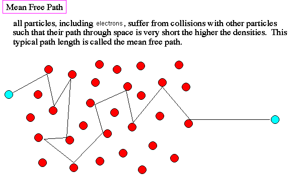
Electron Mean Free Paths
Inelastic interactions of electrons with solids are very important for many measurement techniques such as energy loss spectroscopy, low energy electron diffraction, photoemission spectroscopy and time-resolved two-photon photoemission. The mean free path of an electron (average speed times the scattering time) is the average distance an electron travels between two consecutive scattering events.
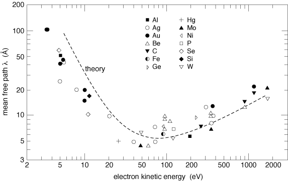
The electron mean free paths are well known in two energy regimes: at high energies, where they are predicted either with Bethe(-like) equations or with the more accurate optical models based on the free-electron-gas approximation, and at very low energies, where they are calculated either with experimental data on electron lifetimes or with first-principles calculations.
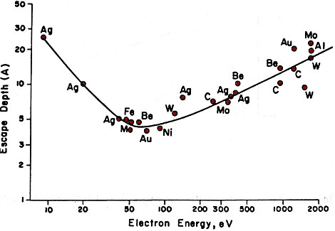
Figs. The inelastic electron mean free path (escape depth) is plotted versus initial kinetic energy.
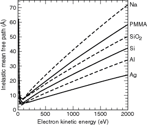
Inelastic mean free paths for electron kinetic energies up to 2000 eV, for Ag, Al, NA, PMMA, Si, and SiO2.
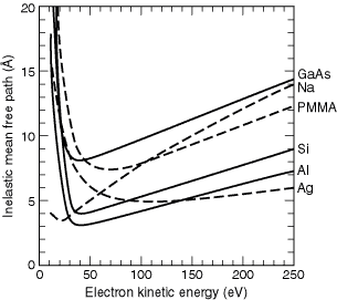
The inelastic mean free paths in the kinetic energy range below 250 eV, for Ag, Al, GaAs, NA, PMMA, and Si.
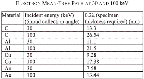
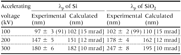
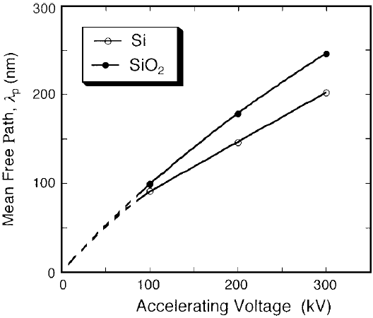
References: Transmission EELS Attachment for SEM, Tao Luo and Anjam Khursheed, IEEE TRANSACTIONS ON DEVICE AND MATERIALS RELIABILITY, VOL. 6, NO. 2, (2006) 182. The electron inelastic mean free path in silicon for 3 keV electron energy is under 50 Å. References: S. Tanuma, C. J. Powel, and D. R. Penn, Surf. Interface Anal. 17, 911 (1991). For Si and Ge, the electron mean free path at an energy of 30 keV is about 20 nm. References: W. Brilnger and W. Menz, Zeit. Phys. 184, 271 (1965). Table Mean Free Path (λp) of Si and SiO2
Referance: Measurement of mean free paths for inelastic electron scattering of Si and SiO2, Journal of Electron Microscopy, C. Lee, Y. Ikematsu and D. Shindo 51(3): 143-148 (2002). Contact us: Feedback |
|
||||||||
|
Copyright (C) 2006 GlobalSino, All Rights Reserved
|