Diffraction Pattern of TEM

http://www.globalsino.com/  


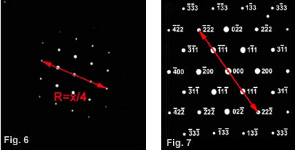
Fig. 6: Electron diffraction pattern from single crystal silicon, with the beam parallel to the [011] zone axis. Fig. 7: Indexing of single crystal silicon diffraction pattern, with the beam parallel to the [011] zone axis.

Diffraction Pattern of TEM


Contact us: Feedback


Procedure of PEELS operation
Limitation of EELS
TEM instruments for HAADF
Operation of EDS
Examples of EDS data
Operation of TEM
Astigmatism of Electron Microscope
Inelastic Scattering of Electrons
Scanning Transmission Electron Microscope (STEM) System
Image mode of TEM
Cubic crystal lattices of sc, bcc and fcc
Resistivity of materials


Copyright (C) 2006 GlobalSino, All Rights Reserved