|
|
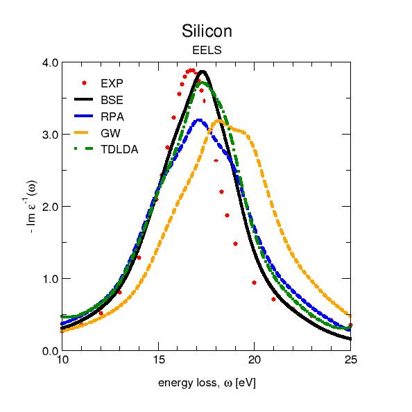
EELS of Silicon
EELS from an amorphous area (silicon rich area)
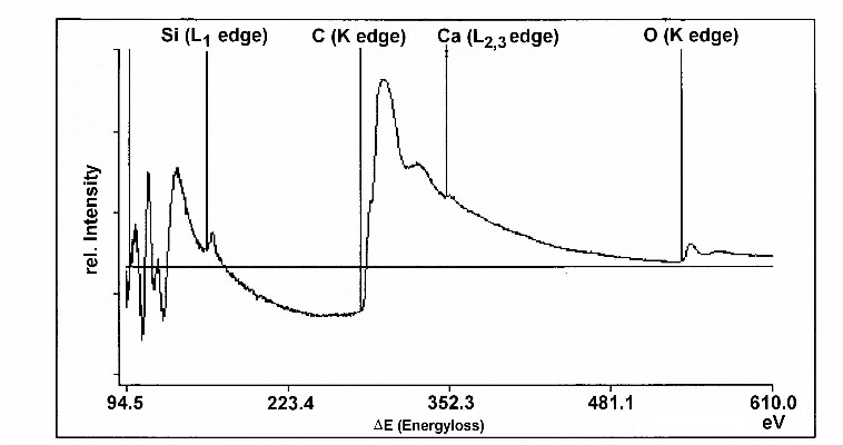
Silicon detection in an algal cell by electron energy loss spectroscopy (EELS)
Mapping overlapping edges using MLLS fitting. The data was acquired by EELS-SI from an etched semi-conductor device (left). The Al K, Si K and W M edges all overlap, prohibiting conventional background extrapolation (centre). Using MLLS fitting,with reference edges extracted from the data-set itself, the signals can be separated without overlap artefacts (right). The MLLS routine can even provide individual maps for the individual Si phases.
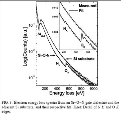
Reference: Compositional analysis of ultrathin silicon oxynitride gate dielectrics by quantitative electron energy loss spectroscopy, Heiko Stegmann and Ehrenfried Zschech, APPLIED PHYSICS LETTERS VOLUME 83, NUMBER 24, 5017 (2003). The Si L2,3 core-loss edge can be used to probe the crystal chemistry around Si, providing information on the s- and d-like partial density of unoccupied states of the Si-O bonds. Shift of ionization edge: In comparison with a bulk Si, this Si edge of GeSi is shifted more than 1 eV towards higher energies and has a different shape. Contact us: Feedback |
|
||||||||
|
Copyright (C) 2006 GlobalSino, All Rights Reserved
|