Electron Dose of Electron Beam - Practical Electron Microscopy and Database - - An Online Book - |
||||||||||||||||||||||||||||||||||||
| Microanalysis | EM Book http://www.globalsino.com/EM/ | ||||||||||||||||||||||||||||||||||||
| ================================================================================= | ||||||||||||||||||||||||||||||||||||
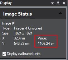
Typical high-dose STEM imaging conditions with a dose of ~1.0 x 10⁸ e-/Å2 are an electron beam current of ~50 pA, a pixel dwell time of 20 µs, and a pixel size of 0.05 Å2. In many cases, e.g. for biological materials, due to specimen damage by the electron beam, low dose needs to be used. The most straightforward method to lower the electron dose is to reduce the pixel dwell time (i.e., increasing the STEM scanning speed). The electron dose on the TEM specimen could not be determined accurately, because of the scattering absorbance surrounding the specimen. However, the electron dose on CCD can be measured precisely on User Interfaces (UI), e.g. DigitalMicrograph (DM) as shown in Figure 1414 .
Figure 1414. Electron dose at a specific pixel shown on DigitalMicrograph (DM). Table 1414 lists examples of dose conditions for various techniques. The low dose of 2.6 × 10³ e-/Å2 in STEM imaging conditions was established by Buban et al. [1] and represents the lowest practicable dose for high resolution HAADF STEM measurement at atomic level. Table 1414. Examples of Dose Conditions for Various Techniques.
[1] Buban, J.; Ramasse, Q.; Gipson, B.; Browning, N.; Stahlberg, H. J.
Electron Microsc. 2010, 59, 103−112.
|
||||||||||||||||||||||||||||||||||||
| ================================================================================= | ||||||||||||||||||||||||||||||||||||
|
|
||||||||||||||||||||||||||||||||||||