|
This book (Practical Electron Microscopy and Database) is a reference for TEM and SEM students, operators, engineers, technicians, managers, and researchers.
|
=================================================================================
Cu (copper) reacts with Si (silicon) rapidly at temperatures ≥ 200 °C. For the systems of Cu/TiN/TiSi2/n+Si - p Si diode junctions, the TiN/TiSi2 bilayer acts as a diffusion barrier between Cu and n+Si layers. In this system, no deterioration of n+-p diode junctions occurs when it is annealed up to 475 °C for 30 min in an N2 ambient. For the sintering temperature at 500 °C, the leakage current increased abruptly and SIMS technique revealed a large amount of Cu atoms diffusing into the junctions of n+-p diodes [2]. The TEM image in Figure 1725 shows that a pyramidal-shaped Cu3Si crystallite in size of 0.25 µm precipitated in the n+Si substrate. The phenomenon is related to Cu penetrating through the TiN/TiSi2 bilayer and reacting with the n+Si substrate to form Cu3Si. [1] The Cu penetration can be induced by lattice diffusion or by diffusion through grain boundaries and defects without reaction with TiN and TiSi2, and then Cu reacts with Si to form Cu3Si crystallite in the n+Si. A gap between TiSi2 and n+Si may be generated during the growth of Cu3Si precipitates, and then the electrical contact resistance is increased. SiO2 can also be found underneath the Cu3Si precipitates. The formation of the SiO2 layer is due to the rapidly catalytic behavior of Cu3Si at room temperature. Because of Cu depletion, voids can form at the interface between Cu and TiN. On the other hand, in the annealed TiN/TiSi2 system (even though annealed in N2), oxygen contents can easily accumulate near the interface between TiN and TiSi2. [1]
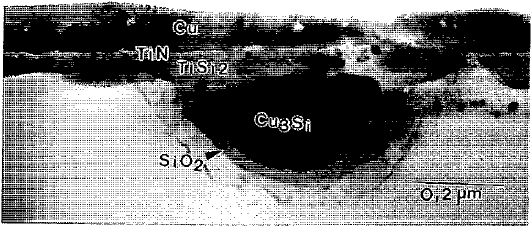
Figure 1725. TEM image of the systems of Cu/TiN/TiSi2/n+Si - p Si diode junctions after sintering at 500 °C/30 min in N2. [2]
[1] A. Cross, M. 0. Aboelfotoh, and K. N. Tu, J. Appl. Phys. 67,332s (1990).
[2] Tzong-Sheng Chang, Wen-Chun Wang, Lih-Ping Wang, Jenn-Chang Hwang, and Fon-Shan Huang, Thermal stability study of TiN/TiSi2 diffusion barrier between Cu and n+Si, J. Appl. Phys. 75 (12), (1994) 7847.
|