|
This book (Practical Electron Microscopy and Database) is a reference for TEM and SEM students, operators, engineers, technicians, managers, and researchers.
|
=================================================================================
Even though the rapid development and applications of copper (Cu) technology, the Al/Ti/W/TiN stack has been widely used for VLSI interconnection [1]. Especially, this stack could be found in most ICs with large fabrication volume before 2008. As a consequence, the thermal stability, electromigration, crystallography, alloys, phases of the Al/Ti/W system have been frequently experimentally and theoretically analyzed.
Figure 2216 (a) shows a typical bright field TEM image of an Al/Ti/W/TiN via after thermal stress at 450 °C for 4 hours. An Al3Ti layer is formed between Al and W via. Figure 2216 (b) shows an EELS profile acquired over 20 s in the needle inclusion. The chemical formula of the needles is between Al10W and Al12W.
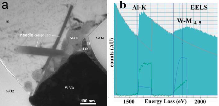
Figure 2216. (a) A typical bright field TEM image of an Al/Ti /W/TiN via after thermal
stress at 450 °C for 4 hours, and (b) The EELS analysis of the needle inclusion. Adapted from [2].
[1] M. Brillouët, MAM’97 Proceedings, SFV, Le Vide, Vol. 283 Suppl., 1997, pp. 36–39.
[2] R. Pantel, H. Wehbe-Alause, S. Jullian, L.F.Tz. Kwakman, A nalytical transmission electron microscopy observation of
aluminium–tungsten interaction in thermally stressed Al/Ti /W/TiN interconnections, Microelectronic Engineering 64 (2002) 91–98.
|