=================================================================================
Conventional TEM specimen preparation is based on cutting the interesting areas from the sample, agglutinating and polishing the obtained blocks to approximately 10 to 15 µm thickness, and ion-milling to create a small hole to have an electron-transparent area around the hole.
The detailed procedure of one specific method of the mechanical polishing techniques is:
i) Cut two blocks from the interesting areas of a sample.
ii) Glue the two blocks together with epoxy, with the interesting surfaces face-to-face, as shown in Figure 2805a.
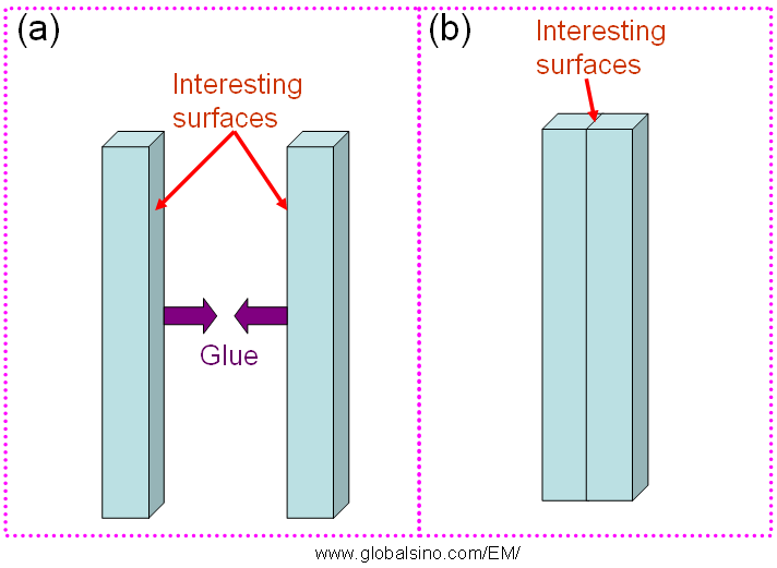
Figure 2805a. Before (a) and after (b) the interesting surfaces are glued face-to-face.
iii) Cut a part of the glued blocks with a diamond saw into small pieces of approximately 1 × 3
mm. Note the reason of why the long side is 3 mm is that the TEM grids are in this dimension.
iv) Agglutinate the glued blocks on a small glass cylinder with wax by heating.
v) Mount the cylinder in a tripod. Figure 2805b shows the top view and bottom view of a tripod.
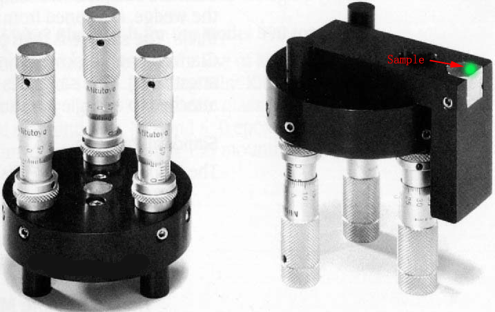
Figure 2805b. The top view (a) and bottom view (b) of a tripod.
The bottom view also shows a sample (indicated in green) attached in the tripod.
vi) Polish the sample with a series of diamond abrasive films with decreasing grain sizes as listed in Table 2805a.
Each polishing step removes the scratches from the previous one. In the final polishing step, silica solution (e.g. Syton HT-50) on a velvet cloth can be used. This step is also called chemical mechanical polishing (CMP). Syton HT-50 produced by Testbourne Ltd. is a solution of colloidal silica with particle sizes in the range of 0.02 to 0.05 µm.
Table 2805a. Mechanical polishing steps with a series of diamond abrasive films with decreasing grain sizes for conventional TEM sample preparation.
Note that some polishing steps (e.g. 9 µm in grain size) can practically be skipped, while the last step with 0.1 µm in grain size should not be skipped.
Grain size [µm] |
30 |
15 |
9 |
6 |
3 |
1 |
0.1 |
In this way, the crystal defects generated in the cutting and polishing steps are removed during thinning the samples.
vii) Detach the specimens from the glass cylinder (polishing stub) once the desired surface quality has been obtained. In this step, the specimens are removed from the polishing stub by dipping in acetone for ~20 minutes.
viii) Attach a ring to the polished surface as shown in Figure 2805c (a).
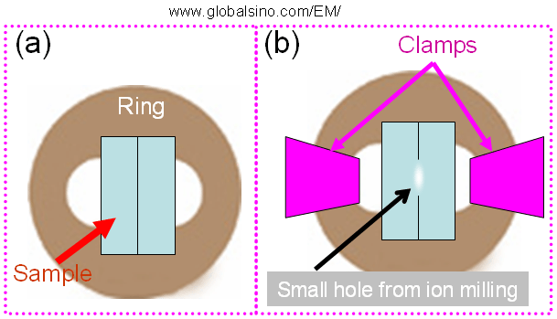
Figure 2805c. (a) A ring attached to the polished surface, and (b) Ion milling to thin down the centre of sample to a few nm, creating a small hole in the middle.
ix) Mount the sample upside down on the glass cylinder again.
x) Polish the second side with the procedure listed in Table 2805b until a total sample thickness of 10 to 15 µm is reached. The polishing steps are the same as described in vi).
Table 2805b. Mechanical polishing steps with a series of diamond abrasive films with decreasing grain sizes for conventional TEM sample preparation.
Note again that some polishing steps can practically be skipped, while the last step with 0.1 µm in grain size should not be skipped.
Polish until thickness [µm] |
100 |
70 |
50 |
35 |
25 |
15 |
15 |
Grain size [µm] |
30 |
15 |
9 |
6 |
3 |
1 |
0.1 |
Some samples can be mechanically polished thinner (or even down to a few hundred nanometres) by monitoring the color change of the transmitted light through the polished thin film. For instance, Table 2805c can be applied to monitor the thickness of mechanically polished Si (silicon) films.
Table 2805c. Correspondence between the Si wafer thickness and color of transmitted light. Note the the incident light is white light.
Si thickness [µm] |
5 |
4 |
3 |
2 |
1 |
Color |
Red |
Reddish-orange |
Orange-red |
Orange |
Light orange |
xi) Similar to step vii), detach the specimen from the polishing stub. The specimen is removed from the polishing stub by dipping in acetone for ~20 minutes.
xii) Insert the sample into a special sample holder in order to allow the Ar+ ions to reach the sample as shown in Figure 2805c (b). In this step, two ion guns mill the sample with 4 keV argon ions at an incident angle of 4° for about five minutes on both sides.
Note that the post-cleaning is critical and essential after colloidal silica polishing. For high quality specimen preparation, plasma cleaning can also be used prior to ion beam milling.
xiii) Once a small hole in the middle becomes visible (also see Figure 2805c (b)), lower energies at higher angles are used to remove the damaged, amorphized layer from the two surfaces.
As an example of TEM sample preparations using mechanical polishing in combination with ion milling, polycrystalline silicon sample was mechanically polished until less than 10 µm in thickness, and then ion milled with 3 keV Ar ions in a Gatan Model691 PIPS. The final thickness for EELS measurements of grain boundaries was 20 nm. [1]
Furthermore, the specimen preparation procedure described above can be applied to both cross-sectional and plan-view TEM.
However, TEM specimen preparation of many materials is challenging because of various reasons for different materials:
i) Cracks initiate very easily for many materials, e.g. glassy materials.
ii) Ion milling causes significant heating due to the low heat conduction of the materials.
Note that for ion-milling materials, contamination can be induced by the back streaming of oil from oil pumped vacuum systems.
On the other hand, electropolishing is a well-known technique, mostly used to prepare (inter)metallic samples, because these materials are conducting, too soft for crushing, and easily damaged by conventional ion milling.
[1] Norihito Sakaguchi, Makito Miyake, Seiichi Watanabe and Heishichiro Takahashi, EELS and Ab-Initio Study of Faceted CSL Boundary in Silicon, Materials Transactions, Vol. 52, No. 3 (2011) 276.
|