=================================================================================
In 2009, ISMI has defined non-visual defects (NVD) as a novel category of process-induced defects in semiconductors that cause electrical failures but are not detected with visual wafer inspection tools.[5] However, with further scaling,
non-visual defects in IC devices are narrowed down to the defects which are invisible under SEM and even TEM. For instance, such defects are leakage of EEPROM Cell junctions across inter-junction spaces [3], blocked LDD (Lightly Doped Drain) implantaion [4], NBTI (Negative Bias Temperature Instability), Intra-level or Inter-level leakage, e.g. in Cu/low k technology, instability with Cu/low k interaction, stress induced leakage current (SILC), trap-assisted gate dielectric leakage current, gate induced drain leakage current, sub-threshold leakage current, interface instability related to high k gate dielectrics, charge migration, short channel effects, interface adhesive problems.
SEM (scanning electron microscopy)-based nanoprobing technique [1] is frequently used to identify the soft failure and non visible defects. This technique provides the capability of operating probe tips in nanometer range to land exactly on top of the individual source, drain and gate tungsten contact, for instance, as shown in Figure 2823. The SEM provides a high-resolution real-time image that facilitates locating the failing device and placing the probe tips. In this way, the locations of soft failure and non visible defects can become visible during electrical stressing.
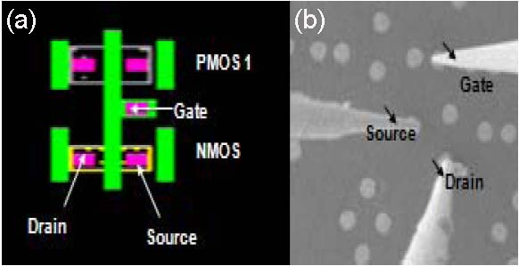
Figure 2823. (a) Inverter image, and (b) A SEM image showing three tungsten probes (black arrow) landing on tungsten contacts of the NMOS transistor in the inverter.
Adapted from [2]
Once the exact failing transistor was successfully located using the Nanoprobing method, Ravikumar et al. [2] had analyzed this transistor using FIB (Focussed Ion Beam), STEM (Scanning Tunneling Electron Microscopy), and TEM (Transmission Electron Microscopy) sequentially one by one. Unfortunately, no physical defects were found using any of those PFA techniques. Therefore, they proposed that the malfunction of the transistor was probably caused by the quality of the extent of implantation which is not detectable in any of those PFA techniques.
[1] D. Faure, C.A. Waggoner, “A New Sub-micron Probing
Technique for Failure Analysis in Integrated Circuits”,
ESREF 2002.
[2] Ravikumar V K, Ho M Y, Goruganthu R R, Phoa S L, Narang V, Chin J M, Combining High Resolution Pulsed TIVA and Nanoprobing Techniques to identify Drive Strength issues in Mixed Signal Circuits, 2010 17th IEEE International Symposium on the Physical and Failure Analysis of Integrated Circuits (IPFA).
[3] Ng Hui Peng, Ang Ghim Boon, Chen Chang Qing, Quah Alfred, Teo Angela, Lee Mern Tat, Indahwan Jony, Zhao Si Ping, Application of AFP in Resolving Systematic Issue in Wafer Fabriation, ISTFA 2013: Proceedings from the 34th International Symposium for Testing and Failure Analysis, San Jose, California, USA.
[4]
Cha-Ming Shen, Tsan-Chen Chuang, Shi-Chen Lin, Lian-Fon Wen, Chen-May Huang, Taiwan Semiconductor Manufacture Company, Combining the Nano-Probing Technique with Mathematics to Model and Identify Non-Visual Failures, ISTFA 2007: Proceedings from the 33rd International Symposium for Testing and Failure Analysis.
[5] Kim Kye-Won, Godwin Milt, Vartanian Victor, Lee Yun Jung, Non Visual Defect (NVD) Workshop, ISMI Project Plans for NVD, Austin, TX, August 27 (2009),
|