|
This book (Practical Electron Microscopy and Database) is a reference for TEM and SEM students, operators, engineers, technicians, managers, and researchers.
|
=================================================================================
In many cases, the difference of voltage contrasts between non-defective (normal) and deflective locations in integrated circuits (ICs) is not significant because of the small deviation of impedance between them, for instance, when the defective plug is amorphous silicon (Si) instead of poly-Si in normal plugs. In these cases, e.g. the case in Figure 2853, interval scan of electron beam can be used to enhance the voltage contrast. Conventional scan employs electron scan without time interval between different scans.
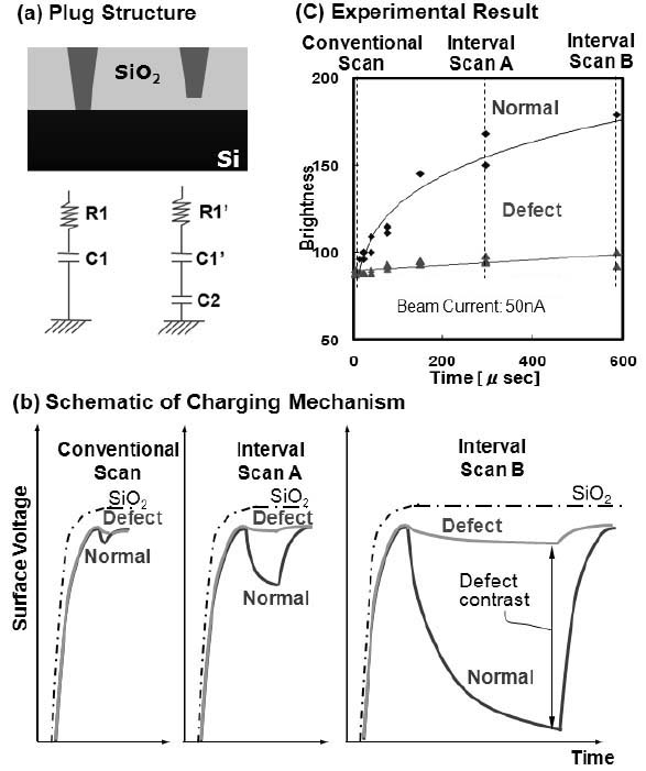
Figure 2853. (a) Schematic diagram of poly-Si plug structures, (b) Schematic diagram of charging mechanism at each scan method, (c) Time-dependent experimental profile of the difference of SEM voltage contrast between normal plug and defective plug. Adapted from [1]
[1] J. H. Oh, G. Kwon, D. Y. Mun, D. J. Kim, I. K. Han, H. W. Yoo, J. C. Jo, Y. Ominami, T. Ninomiya, and M. Nozoe, Interval Scan Inspection Technique for Contact Failure of Advanced DRAM Process using Electron Beam-Inspection System, Journal of Semiconductor Technology And Science, 12 (1) (2012) 34.
|