=================================================================================
Contrast reversal
by defocus is well-known in conventional TEM imaging. For a modern uncorrected 300-kV TEM with Cs = 0.6 mm and an information limit of 0.1 nm, the actual point resolution is only 0.17 nm and the smallest delocalization is up to even 1.2 nm! [2] For an uncorrected TEM operated at Scherzer defocus, rapid contrast reversals happens at spatial frequencies between the Scherzer limit and the information limit, making the interpretation of the images very difficult.
Lichte defocus of least confusion minimizes contrast delocalization, however, the strong spherical aberration under this condition induces the poor point resolution and the contrast reversals in the entire frequency range.
Based on the optical reciprocity theorem [3], BF-STEM images can be related to the HRTEM images of an atom as a phase object. Like HRTEM images, BF-STEM images are very sensitive to the focal conditions, and contrast reversal is often observed because of multiple scattering and phase shift due to defocus condition of the lens. A full interpretation of BF-STEM images can be done with phase contrast simulation in the same way as the HRTEM images. [4]
The elements with larger atomic number (Z) has stronger elastic and thermal diffuse scattering and thus, a solid composed of element with larger Z can have larger mean free path value λ, i.e. weaker inelastic scattering. As an example, Figure 2881 shows the bright- and dark-field STEM images of a diamond/Si interface taken from a thick specimen. Note that the thick specimen is used in order to have multiple inelastic events as dominated scattering. The diamond area appears darker than Si in both dark- and bright-field images, different from the common cases. It is important to mention that in general this phenomenon, showing contrast reversal in the bright-field image, could cause misinterpretations of bright-field images of mixed-phase specimens where the spatial distribution of different materials is unknown.
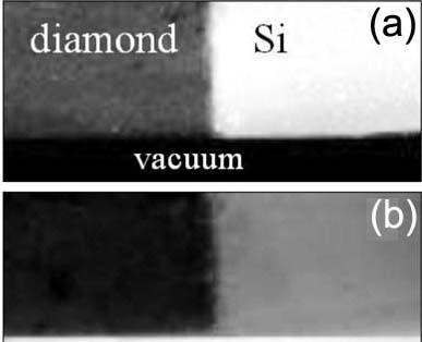
| Figure 2881. Dark-field (a) and bright-field (b) STEM images of a diamond/Si interface taken from a thick specimen (Zdiamond = 6 and ZSi = 14).
Adapted from [1] |
[1] Konstantin Iakoubovskii, Kazutaka Mitsuishi,Yoshiko Nakayama, and Kazuo Furuya, Mean free path of inelastic electron scattering in elemental solids and oxides using transmission electron microscopy: Atomic number dependent oscillatory behavior, Physical Review B 77, 104102 (2008).
[2] Markus Lentzen, Progress in Aberration-Corrected High-Resolution Transmission Electron Microscopy Using Hardware Aberration Correction, Microsc. Microanal. 12, 191–205, 2006.
[3] Born M, Wolf E. Principles of optics. Cambridge, UK: Cambridge University Press; 1997.
[4] Spence JCH. High resolution electron microscopy. 3rd ed. Oxford: Clarendon Press; 2003.
|