| The surface and bulk plasmon energies in EELS can be theoretically modeled or measured experimentally. In general, Table 4623a lists the trend of inelastic mean
free paths (λ) under different experimental conditions.
Table 4623a. Trend of inelastic mean
free paths (λ) under different experimental conditions. |
| |
Accelerating voltage of the electron beam (V) |
Collection semi-angle (β) |
High |
Low |
Large |
Small |
| Mean
free path |
Large |
Small |
Small |
Large |
Table 4623b lists bulk plasmon energies, full-width-at-half-maximum of bulk plasmon energies, bulk plasmon mean free path, and inelastic mean free path of some common elements and compounds, as well as their crystal structure (Notation: a for amorphous, b for body-centered cubic, c for cubic, f for face-centered cubic, h for hexagonal, l for liquid, o for orthorhombic, r for rhombohedral, t for tetragonal) [1 - 6].The bulk plasmon mean free path λp represents the collective valence electron component of inelastic scattering. The differences between λp and λi reflect single-electron excitation, for example, an inner-shell ionization edge occurring below 150 eV. In addition, Table 4623b also lists surface plasmon energies (Es) of some elements and components. Note that the accuracies are ~5%–10% for λ and ~10%–30% for λp. [16]
For specific experimental conditions or structures of materials, the plasmon energies are slightly affected by many factors:
i) Plasmon energies slightly depend on the incident beam energy. In EELS measurement, the decrease of electron-beam energy gives rise to a low energy shift and a widened
plasmon peak.
ii)
The energies of plasmon peaks can be lowered by defect excitations or interband transitions.
Table 4623b. Surface plasmon energies (Es), bulk plasmon energies (Ep in eV), full width at half-maximum Ep (ΔEp), bulk plasmon mean free path (λp in nm), elastic mean free path (λe in nm), approximate bulk plasmon mean free path obtained by theoretical calculation (λapp in nm), and inelastic mean free path (λi in nm)
at different incident kinetic energies (λi3, λi30, λi100, λi200, and λi300 at incident kinetic energies of 3 keV, 30 keV, 100 keV, 200 keV, and 300 keV, respectively). Note: for some elements, the table lists multiple values gathered from different references. |
|
Es , eV |
ΔEp, eV |
|
Origin
of Ep |
λe, nm |
|
|
|
|
λapp, nm |
λp, nm** |
Ag (f) |
3.7 |
|
25 |
|
|
|
|
100 |
|
|
125 |
Ag (poly-c) |
|
|
|
|
|
|
71 (β = 10-100 mrad) [20] |
|
|
|
|
Ag2O |
|
|
|
|
|
|
|
112 |
|
|
|
|
10.3[7,8] |
|
|
|
|
λi30=55.5 |
|
134 |
|
155 |
160 |
Al (c) |
|
|
~15 |
|
|
|
100 (β = 10-100 mrad) [17] |
|
|
|
|
Al (poly-c) |
|
|
|
|
|
|
101 (β = 10-100 mrad) [18] |
|
|
|
|
AlAs |
|
|
16.1 |
|
|
|
|
|
|
146 |
|
Al2O3 (α) |
|
10 - 20 |
22.2-26[9-12] |
|
|
|
|
130-140 |
|
109 |
|
Al2O3 (poly-c) |
|
|
|
|
|
|
106 (β = 10-100 mrad) [19] |
|
|
|
|
As (r) |
|
|
18.7 |
|
|
|
|
|
|
129 |
|
As (a) |
|
|
16.7 |
|
|
|
|
|
|
142 |
|
|
|
|
|
|
|
λi30=38 |
|
|
|
|
|
Au (poly-c) |
|
|
|
|
|
|
56 (β = 10-100 mrad) [20] |
|
|
|
|
Au (f) |
~1 |
|
24.8 |
|
|
|
|
84 |
|
|
120 |
B(a) |
|
18 |
22.7 |
|
|
|
|
123 |
|
110 |
126 |
Ba (b) |
|
7.5 |
27.8 |
|
|
|
|
|
|
94 |
|
BaO |
|
|
27.6 |
|
|
|
|
125 |
|
|
|
Be (c) |
12–14 |
|
19.2 |
|
|
|
129 (β = 10-100 mrad) [17] |
|
|
|
|
Be(h) |
|
4.8 |
18.7 |
|
|
|
|
160 |
|
129 |
169 |
Be3N2
|
|
|
23 |
|
|
|
|
|
|
|
|
Bi (r) |
|
6.5 |
14.2 |
|
|
|
|
105 |
|
162 |
147 |
Bi2O3 |
|
|
|
|
|
|
|
125 |
|
|
|
BN (h) |
|
|
9 & 26 |
|
|
|
|
|
|
|
|
BN (a) |
|
|
24 |
|
|
|
|
|
|
|
106 |
BN (c) |
|
|
|
|
|
|
99 (β = 10-100 mrad) [21] |
|
|
|
|
B2O3 |
|
|
|
|
|
|
|
120 |
|
|
|
|
|
|
|
|
|
λi30=67 |
|
|
|
|
|
C (diamond) |
|
13 |
33.2 |
|
|
|
88 (β = 10-100 mrad) [19] |
112 |
|
81 |
116 |
DLC |
|
|
27 |
|
|
|
|
|
|
|
|
C (graphite) |
|
|
23~25 |
|
|
|
|
|
|
|
|
C (a) |
|
20 |
24 |
|
|
λi40=34 |
74 |
116-160 |
24.5 eV |
|
106 |
C (C60) |
|
|
|
|
|
|
115 (β = 10-100 mrad) [19] |
|
|
|
|
Ca (f) |
|
2.1 |
8.8 |
|
|
|
|
|
|
241 |
|
CaO |
|
|
|
|
|
|
|
130 |
|
|
|
Cd (h) |
|
|
|
|
|
|
|
107 |
|
|
130 |
Ce2O3 |
|
|
|
|
|
|
|
125 |
|
|
|
|
|
|
|
|
|
|
|
|
|
|
|
Co (h) |
|
|
20.9 |
|
|
|
|
98 |
|
118 |
108 |
CoO |
|
|
24.6 |
|
|
|
|
115 |
|
|
|
Cr (b) |
|
|
24.9 |
|
|
|
|
104 |
|
102 |
149 |
Cr (poly-c) |
|
|
|
|
|
|
74 (β = 10-100 mrad) [19] |
|
|
|
|
Cr2O3 |
|
|
|
|
|
|
|
118 |
|
|
|
Cs (b) |
|
|
2.9 |
|
|
|
|
|
|
175 |
|
|
|
|
|
|
|
λi30=46.4 |
|
|
|
|
|
Cu (f) |
|
|
19.3 |
|
|
|
|
100 |
|
126 |
100 |
Cu (poly-c) |
|
|
|
|
|
|
63 (β = 10-100 mrad) [18] |
|
|
|
|
Dy (h) |
|
|
|
|
|
|
|
118 |
|
|
310 |
Dy2O3 |
|
|
|
|
|
|
|
126 |
|
|
|
Er (h) |
|
|
14 |
|
|
|
|
|
|
|
|
Er2O3 |
|
|
|
|
|
|
|
115 |
|
|
|
Eu2O3 |
|
|
|
|
|
|
|
118 |
|
|
|
Fe (b) |
|
|
23 |
|
|
|
|
102 |
|
109 |
121 |
Fe (poly-c) |
|
|
|
|
|
|
74 (β = 10 mrad); 57 (β = 100 mrad) [18, 20] |
|
|
|
|
Fe (306 stainless steel) |
|
|
|
|
|
|
78 (β = 10 mrad); 61 (β = 100 mrad) [17] |
|
|
|
|
Fe2O3 |
|
|
21.8 |
|
|
|
|
116 |
|
|
|
Ga |
|
0.6 |
13.8 |
|
|
|
|
|
|
166 |
|
GaAs (c) |
|
|
15.8 |
|
|
|
95 (β = 10 mrad); 74 (β = 100 mrad) [19] |
|
|
148 |
|
GaN |
|
|
19.4 |
|
|
|
|
|
|
|
|
GaP |
|
|
16.5 |
|
|
|
|
|
|
143 |
|
GaSb |
|
|
13.3 |
|
|
|
|
|
|
171 |
|
|
|
|
16.0 |
|
|
λi30=~ 20 |
|
|
|
|
|
Ge (c) |
|
|
15.8 |
|
|
|
|
120-140 |
|
148 |
126 |
GeO2 |
|
|
|
|
|
|
|
130 |
|
|
|
Gd (h) |
|
|
|
|
|
|
|
110 |
|
|
275 |
Gd2O3 |
|
|
14.6 |
|
|
|
|
125 |
|
158 |
|
Hf (h) |
|
|
|
|
|
|
|
95 |
|
|
237 |
Hf (c) |
|
|
|
|
|
|
57 (β = 10 mrad); 41 (β = 100 mrad) [17] |
|
|
|
|
|
|
|
|
|
87 at 300 keV |
|
|
~112 |
95 [20 mrad] |
|
|
Hg (l) |
|
1 |
6.4 |
|
|
|
|
|
|
|
|
HgO |
|
|
|
|
|
|
|
116 |
|
|
|
H2O (c) |
|
|
|
|
|
|
220 (β = 10 mrad); 200 (β = 100 mrad) [19, 22] |
|
|
|
|
Ho2O3 |
|
|
|
|
|
|
|
120 |
|
|
|
I (o) |
|
|
|
|
|
|
|
140 |
|
|
233 |
In (t) |
|
12 |
11.4 |
|
|
|
|
110 |
|
|
129 |
InSb |
|
|
12.9 |
|
|
|
|
|
|
|
|
Ir (b) |
|
|
|
|
|
|
|
78 |
|
|
121 |
IrO2 |
|
|
29 |
|
|
|
|
110 |
|
|
|
La2O3 |
|
|
|
|
|
|
|
130 |
|
|
|
|
|
|
|
|
|
|
|
|
|
|
|
Li (b) |
|
2.2 |
7.1-7.4 |
|
|
|
|
|
|
289 |
|
LiH |
|
|
20.9 |
|
|
|
|
|
|
118 |
|
LiF |
|
|
24.6 |
|
|
|
|
|
|
103 |
|
Li12Si7 |
|
|
14.1 |
|
|
|
|
|
|
|
|
Li7Si3 |
|
|
13.6 |
|
|
|
|
|
|
|
|
Li13Si4 |
|
|
13.1 |
|
|
|
|
|
|
|
|
Li22Si5 |
|
|
12.9 |
|
|
|
|
|
|
|
|
Mg (h) |
|
0.7 |
10.3 |
|
|
|
|
150 |
|
211 |
214 |
MgB2 |
|
|
18.9 |
|
|
|
|
|
|
|
|
MgF2 |
|
|
24.6 |
|
|
|
|
|
|
103 |
|
MgO |
|
|
22.3 |
|
|
|
93 |
133 |
152 |
112 |
|
Mn (c) |
|
|
21.6 |
|
|
|
|
106 |
|
115 |
146 |
Mo (b) |
|
|
25.2 |
|
|
|
|
98 |
|
|
163 |
MoO3 |
|
|
24.4 |
|
|
|
|
111 |
|
|
|
Na (b) |
|
0.4 |
5.7 |
|
|
|
|
|
|
348 |
|
NaCl |
|
|
15.5 |
|
|
|
|
|
|
151 |
|
Nb (b) |
|
|
|
|
|
|
|
105 |
|
|
194 |
NbC |
|
|
24.0 |
|
|
|
|
|
|
|
|
Nd2O3 |
|
|
14.2 |
|
|
|
|
120 |
|
162 |
|
Ni (f) |
|
|
20.7 |
|
|
|
|
98 |
|
119 |
103 |
NiO |
|
|
22.6 |
|
|
|
|
115 |
|
111 |
|
NiO (c) |
|
|
|
|
|
|
89 (β = 10 mrad); 71 (β = 100 mrad) [17] |
|
|
|
|
NiSi2 |
|
|
19.75 - 20.0 |
|
|
|
|
|
|
|
|
NiSi |
|
|
20.25 - 20.7 |
|
|
|
|
|
|
|
|
Ni2Si |
|
|
21.9 |
|
|
|
|
|
|
|
|
|
|
|
|
|
|
|
|
|
|
100 |
|
P (o) |
|
|
|
|
|
|
|
160 |
|
|
160 |
Pb (f) |
|
|
13 |
|
|
|
|
99 |
|
|
141 |
PbO |
|
|
|
|
|
|
|
122 |
|
|
|
Pd (b) |
6.5[13] |
|
25.1&31.9[13] |
|
|
|
|
94 |
|
|
118 |
PdO |
|
|
3.7&7.6[13] |
|
|
|
|
110 |
|
|
|
Pr2O3 |
|
|
|
|
|
|
|
122 |
|
|
|
Pt (b) |
|
|
22.6 |
|
|
|
|
82 |
|
111 |
120 |
Rb (b) |
|
0.6 |
3.41 |
|
|
|
|
|
|
539 |
|
Re (h) |
|
|
28 |
|
|
|
|
78 |
|
|
141 |
Ru (b) |
|
|
|
|
|
|
|
90 |
|
|
134 |
S (o) |
|
|
|
|
|
|
|
200 |
|
|
200 |
Sb (r) |
|
3.3 |
15.2 |
|
|
|
|
120 |
|
145 |
234 |
Sc (h) |
|
|
14 |
|
|
|
|
|
|
604 |
|
Sc2O3 |
|
|
|
|
|
|
|
125 |
|
|
|
Se (h) |
|
6.2 |
17.1 |
|
|
|
|
130 |
|
|
205 |
Se (a) |
|
6.2 |
16.3 |
|
|
|
|
|
|
145 |
|
SeO2 |
|
|
3.95 |
|
|
|
|
130 |
|
|
|
|
|
|
|
|
|
λi3< 5; λi30=~ 20; λi1.5=2.11; λi0.15=0.4
|
|
|
|
|
|
Si (c) |
8.2 |
3.2 |
16.7 |
Si 2p |
|
|
111 (β = 10 mrad); 91 (β = 100 mrad) [20] |
145 |
|
142 |
168 |
Si (a) |
|
3.9 |
16.3 |
|
|
|
|
|
|
145 |
|
SiC (α) |
|
3.9 |
21.5 |
|
|
|
|
|
|
|
|
Si3N4 (α) |
|
10.1 |
23.7 |
N 1s |
|
|
|
|
|
|
|
SixNy (with excess
Si) |
|
|
17 - 24 [25,26] |
|
|
|
|
|
|
|
|
Si3N4/wet SiO2 interface |
|
|
21-22 [23] |
|
|
|
|
|
|
|
|
Si3N4/native oxide interface |
|
|
19.6-20 [24] |
|
|
|
|
|
|
|
|
SiO2 (α) |
|
16.6 |
22.4 |
O 1s |
|
λi1.5=2.96; λi0.15=0.7 |
119 (β = 10 mrad); 99 (β = 100 mrad) [19] |
155 |
|
112 |
|
|
|
|
|
|
660 at 300 keV |
|
|
|
247 [10 mrad], 140 [20 mrad]
|
|
|
Sm (r) |
|
|
|
|
|
|
|
112 |
|
|
280 |
Sm2O3 |
|
|
13.5 |
|
|
|
|
120 |
|
|
|
Sn (t) |
10 |
1.3 |
13.7 |
|
|
λi0.1= 0.7, λi2= 1.0, λi4 = 1.4, λi6= 1.6 [14] |
|
115 |
|
167 |
273 |
SnO |
|
|
|
|
|
λi0.1 = 1.0, λi2 = 1.4, λi4 = 1.9, λi6 = 2.3 [14] |
|
|
|
|
|
SnO2 |
|
|
|
|
|
λi1 = 1.0, λi2 = 1.4, λi4 = 1.9, λi6 = 2.3 [14] |
|
115 |
|
|
|
Sr (b) |
|
2.3 |
8 |
|
|
|
|
|
|
261 |
|
SrO |
|
|
32 |
|
|
|
|
126 |
|
|
|
SrTiO3 |
|
|
|
|
|
|
|
115[15] |
|
|
|
Ta (b) |
|
|
|
|
|
|
|
88 |
|
|
183 |
TaC |
|
|
22.4 |
|
|
|
|
|
|
|
|
Tb (h) |
|
|
13.3 |
|
|
|
|
|
|
|
|
Tb2O3 |
|
|
|
|
|
|
|
125 |
|
|
|
Te (h) |
|
6.2 |
17.1 |
|
|
|
|
130 |
|
|
216 |
Ti (h) |
|
|
17.9 |
|
|
|
|
120 |
|
134 |
202 |
|
|
|
|
|
|
|
|
~140 |
|
|
|
TiO |
|
|
|
|
|
|
|
120 |
|
|
|
Tl (h) |
|
|
|
|
|
|
|
95 |
|
|
135 |
V (b) |
|
|
21.8 |
|
|
|
|
109 |
|
114 |
158 |
Vacuum*** |
|
|
|
|
|
|
|
50 meters |
|
|
|
VC |
|
|
22.2 |
|
|
|
|
|
|
|
|
V2O5 |
|
|
|
|
|
|
|
116 |
|
|
|
W (b) |
|
|
|
|
|
|
|
82 |
|
|
151 |
WO3 |
|
|
|
|
|
|
|
110 |
|
|
|
Y (h) |
|
7 |
12.5 |
|
|
|
|
124 |
|
|
354 |
Yb (f) |
|
|
|
|
|
|
|
110 |
|
|
275 |
Yb2O3 |
|
|
|
|
|
|
|
115 |
|
|
|
YH2 |
|
|
15.3 |
|
|
|
|
|
|
|
|
Y2O3 |
|
|
5.01 |
|
|
|
|
122 |
|
|
|
Zn (h) |
|
|
17.2 |
|
|
|
|
106 |
|
138 |
106 |
ZnO |
16 |
|
|
|
|
|
|
|
|
|
|
Zr (h) |
|
|
|
|
|
|
|
113 |
|
|
268 |
Zr (c) |
|
|
|
|
|
|
75 (β = 10 mrad); 57 (β = 100 mrad) [17] |
|
|
|
|
ZrO2 |
|
|
|
|
|
|
|
115 |
|
|
|
Epon |
|
|
|
|
|
|
|
|
21.5 eV |
|
|
* λi presents the inelastic mean free paths at uncommon accelerating voltages of the electron beam. The applied voltages are noted by x in λix (x is in unit of keV), e.g. λi0.1 is the mean free path of an incident electron at an accelerating voltage of 0.1 keV, namely 100 eV.
** λp gives an approximate value of the bulk plasmon mean free path (which is normally equal to an approximate inelastic mean free path).
*** Vacuum of 10-4 Torr (10100 air molecules/cm3).
**** β presents collection semi-angle.
***** c and
poly-c represent single-crystal and polycrystalline films, respectively. |
In the applications of material science and engineering, the incident electron beam in TEMs used for EELS analysis is normally accelerated to 200 keV. Therefore, the bulk plasmon mean free path (λi200) at such incident kinetic energies is generally in the range of ~80 and 200 nm. Figure 4623 shows a clear periodic dependence of λi200 such that within one row of the Periodic Table, the minimum (maximum) of λi200 is observed for the elements with completed (empty) outer d shell. The oxides present a smaller variation.
For oxides, the atomic number Z corresponds to the main element, e.g., Z=14 for SiO2.
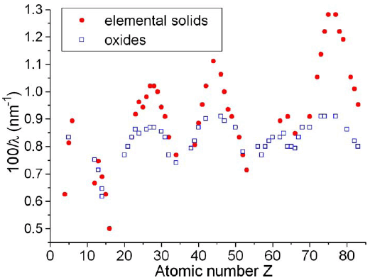
Figure 4623. Periodic dependence of λi200 on
atomic number Z.
[16]
[1] Daniels, J., Festenberg, C. V., Raether, H., and Zeppenfeld, K. (1970) Optical constants of solids by electron spectroscopy. In Springer Tracts in Modern Physics, ed. G. Hoehler, Springer, New York, NY, Vol. 54, pp. 78–135.
[2] Colliex, C., Cosslett, V. E., Leapman, R. D., and Trebbia, P. (1976) Contribution of electron energy-loss spectroscopy to the development of analytical electron microscopy. Ultramicroscopy 1, 301–315.
[3] Raether, H. (1980) Excitation of Plasmons and Interband Transitions by Electrons. Springer Tracts in Modern Physics, Springer, New York, NY, Vol. 88.
[4] Colliex, C. (1984) Electron energy-loss spectroscopy in the electron microscope. In Advances in Optical and Electron Microscopy, eds. V. E. Cosslett and R. Barer, Academic, London, Vol. 9, pp. 65–177.
[5] Ahn, C. C., ed. (2004) Transmission Electron Energy Loss Spectrometry in Materials Science and the EELS Atlas, Wiley, New York, NY.
[6] Iakoubovskii, K., Mitsuishi, K., Nakayama, Y., and Furuya, K. (2008) Thickness measurements with electron energy loss spectroscopy. Microsc. Res. Tech. 71, 626–631.
[7] C.J. Powell, J.B. Swan, (1959) Phys. Rev. 115, 869.
[8] E.D. Johnson, R.P. Merrill, (1985) J. Vac. Sci. Technol. A3, 1313.
[9] C.J. Powell, J.B. Swan, (1960) Phys. Rev. 118, 640.
[10] E.D. Johnson, R.P. Merrill, (1985) J. Vac. Sci. Technol. A3, 1313.
[11] G. Gergely, M. Menyhard, A. Sulyok, (1986) Vacuum 36, 471.
[12] S.D. Berger, I.G. Salisbury, R.H. Milne, D. Imeson, C.J. Humphreys,
(1978) Philos. Mag. B55, 341.
[13] Helena A.E. Hagelin, Jason F. Weaver, Gar B. Hoflund, Ghaleb N. Salaita, Electron energy loss spectroscopic investigation of palladium metal
and palladium(II) oxide, Journal of Electron Spectroscopy and Related Phenomena 124 (2002) 1–14.
[14] Gar B.Hoflund and Gregory R. Corallo, Electron-energy-loss study of the oxidation of polycrystalline tin, Phys. Rev. B 46, 7110–7120 (1992).
[15] R.E. Egerton, Electron Energy-Loss Spectroscopy in the Electron Microscope, Plenum Press, New York, 1996, p. 302.
[16] Konstantin Iakoubovskii, Kazutaka Mitsuishi,Yoshiko Nakayama, and Kazuo Furuya, Mean free path of inelastic electron scattering in elemental solids and oxides using transmission electron microscopy: Atomic number dependent oscillatory behavior, Physical Review B 77, 104102 (2008).
[17] Malis, T., Cheng, S. C., and Egerton, R. F. (1988) EELS log-ratio technique for specimen-thickness
measurement in the TEM. J. Electron Microsc. Tech. 8, 193–200.
[18] Crozier, P. A. (1990) Measurement of inelastic electron scattering cross-sections by electron
energy-loss spectroscopy. Philos. Mag. 61, 311–336.
[19] Egerton, R. F. (1992) A data base for energy-loss cross sections and mean free paths. In 50th Ann.
Proc. Electron Microsc. Soc. Am., San Francisco Press, San Francisco, CA, pp. 1264–1265.
[20] Egerton, R. F., and Cheng, S. C. (1987) Measurements of local thickness by electron energy-loss
spectroscopy. Ultramicroscopy 21, 231–244.
[21] Egerton, R. F. (1981) The range of validity of EELS microanalysis formulae. Ultramicroscopy 6,
297–300.
[22] Sun, S., Shi, S., and Leapman, R. (1993) Water distributions of hydrated biological specimens by
valence electron energy loss spectroscopy. Ultramicroscopy 50, 127–139.
[23] V. A. Gritsenko, S. N. Svitasheva, I. P. Petrenko, Hei Wong, J. B. Xu, and I. H. Wilson, Study of Excess Silicon at Si3N4/Thermal SiO2 Interface Using EELS and Ellipsometric Measurements,
Journal of The Electrochemical Society, 146 (2) 780-785 (1999), S0013-4651(98)06-067-4.
[24]
V. G. Lifshiz, V. G. Kotlar, and A. A. Saranin, Surface (Soy.), 12, 76 (1984).
[25] M. M. Guraya, H. Ascolani, G. Zampiery, J. I. Cisneros, J. H. Diasda Silva, and M.
P. Cantao, Phys. Ref. B, 49, 5677 (1990).
[26] R. Karcher, L. Ley, and R. L. Johnson, Phys. Rev. B, 30, 1896 (1984).
|
