| HfO2 has a
high melting point, high chemical stability, and a large dielectric
constant. Cubic HfO2 modifies the fluorite-type crystal structure with 4 Hf and 8 O atoms occupying the (000) and (0.25 0.25 ±0.25) sites in the fcc unit cell, respectively. Figure 2069a shows the phase transformation of HfO2 with increasing temperature.

Figure 2069a. Phase transformation of HfO2 with increasing temperature.
Table 2069a. Properties of undoped HfO2.
|
Amorphous |
|
|
|
Occurrence |
|
Most common, stable at
low
temperatures |
Stabilized only above 1720 °C |
Stabilized only above 2600 °C |
Lattice parameter (Å) & unit cell volume (V, Å3) |
|
a = 5.124, b = 5.176, c = 5.276, β = 98.94°, V = 138.28 |
a = 3.63; c = 5.25 |
a = 5.08 |
Polymorphism |
Monoclinic-tetragonal: 1893-1923; Tetragonal-cubic: 2973; Cubic-liquid: 3173 |
Density (kg/m3) |
|
9680 |
1001 |
|
Thermal expansion coefficient (10-6 K-1) |
|
5.8 |
|
|
Heat of formation (kJ mol-1) |
-1145.29 |
Boiling point (K) |
4700 |
Mohs hardness |
6.5 |
Space group |
|
P21/c |
P42/mnm, P42/nmc (137) |
Fm-3m (225) |
Static dielectric constant (K) |
25 |
20 |
70 |
30 |
Band gap energy (eV) |
5.8 |
|
|
|
|
1.4 |
|
|
|
|
4.8 for NbSiN, 4.9 for NbN, 4.4-4.5 for TaSiN, 4.34-4.8 for TaN, 4.75-4.8 for HfN |
Effective electron masses (me/m0) |
|
A-B: 1.03; B-D: 1.21 |
M-Γ: 0.72; Γ-Z: 0.94 |
L-Γ: 0.86 & 0.86; Γ-X: 1.97 & 0.68 |
Effective hole masses (mh/m0) |
|
Z-Γ: 0.85; Γ-Y: 1.28 |
Z-A: 0.78 & 0.78; A-M: 8.26 & 8.26 |
Γ-X:0.32; X-W:3.04 |
Notes |
Amorphous with oxygen vacancies |
|
|
|
|
[4] |
[19] |
|
|
Doping tunes the properties of materials. Certain dopants in hafnia tabilize
either the cubic or tetragonal phase over the monoclinic phase at low temperatures. However, it was also found that dopants with small ionic radii easily stabilize the tetragonal phase and dopants with large ionic radii (e.g. Gd, Dy, and Er) stabilize the cubic phase better. The dielectric properties of the films are related to the degree of crystallinity, crystal structure, crystallographic orientation, as well as their stoichiometric composition.
Table 2069b. Characteristics of impurity-doped HfO2.
| Impurity |
Factors affecting formation |
Space group |
Structure |
Lattice parameter (Å) & unit cell volume (Å3) |
Dielectric constants |
Applications |
Notes |
Reference |
| Alkaline-earth & rare-earth doped |
|
|
Stabilized in cubic or tetragonal phases at room temperature |
|
Increase
dramatically compared to undoped m-HfO2 |
|
Deep vacancy trapping is responsible for the decrease in
the ionic conductivity at high dopant concentrations |
[23] |
| Al |
Al ≤ 1.4% & annealing conditions |
Pbc21 (29) |
Non-centrosymmetry |
|
|
Ferroelectric, piezoelectric, pyroelectric |
|
[1] |
| Al |
Al ≤ 1.4% & annealing conditions |
|
Monoclinic |
|
20–25 |
|
Oxygen vacancies play a key role as electron trap centers. Electron trapping and de-trapping leads to resistive switching. Formation of Hf-O-Al bonding reduces the oxygen vacancy formation energy. |
[3, 24] |
| Al |
2.0% ≤ Al ≤ 3.5% |
|
Tetragonal /cubic |
|
30–35 |
|
|
[3] |
| Al |
Al content & annealing conditions |
|
|
|
|
Antiferroelectric |
|
[1] |
| Al |
Al > 4.7% |
|
Amorphous |
|
20 ~ 25 |
|
|
[3] |
| Ce |
Low Ce doping |
|
Monoclinic |
|
|
|
|
[4] |
| Ce |
High Ce doping |
|
Cubic |
|
|
|
|
[4] |
| Ce |
Ce 12.5 at. % |
|
Tetragonal |
|
|
|
|
[21] |
| Co |
|
|
|
|
|
Paramagnetic |
|
[14] |
| Co |
|
|
|
|
|
Ferromagnetic |
|
|
| Er |
|
|
Monoclinic to cubic |
|
|
|
|
|
| Eu |
|
P21/c (14) |
Monoclinic |
a = 5.139, b = 5.186, c = 5.311, β = 99.75°, V = 139.54 |
|
|
|
[19] |
| Gd |
|
|
|
|
23.1 ~ 31.6 |
|
|
[5] |
| Gd |
Lower Gd contents |
P21/c (14) |
Monoclinic with occurrence of orthorhombic phase at the phase boundary |
|
|
|
|
[6] |
| Gd |
Gd at
10 ~ 20% |
Fm-3m (225) |
Cubic |
|
|
|
|
[6, 11] |
| Gd |
Gd > ~15 % |
P42/nmc (137) |
Tetragonal |
|
|
|
Oxygen vacancy formation energy for doped HfO2 is ~ 3 eV lower than un-doped one. |
[6, 26] |
| Gd |
|
Pbc21 (29) |
Non-centrosymmetric, orthorhombic |
|
|
Ferroelectric |
TiN top electrode enhances ferroelectric properties |
[6] |
| Ge |
Ge at 5 % |
|
Tetragonal |
|
|
|
|
[25] |
| Dy |
|
|
Cubic/ tetragonal |
|
|
|
|
[7, 8] |
| Hf |
|
|
|
|
|
|
The hydrophobicity is changed into hydrophilicity |
[27] |
| La |
8% La |
|
Cubic |
|
38 |
|
|
|
| |
|
Orthorhombic |
|
|
Ferroelectric |
|
[53] |
| Mn |
Mn at
10 ~ 20% |
|
Cubic |
|
|
|
Ferromagnetic
and
half-metallic |
[10] |
| Si |
Si content & annealing conditions |
|
Monoclinic |
|
|
|
Monoclinic phase is obtained if the film is not capped |
[1, 28] |
| Si |
|
|
Metastable tetragonal |
|
30 |
Antiferroelectric |
|
[20] |
| Si |
|
|
Cubic |
|
30 |
|
|
[20] |
| Si |
Si at 4 mol.% |
Pbc21 (29) |
Orthorhombic |
|
|
Ferroelectric |
Monoclinic phase is inhibited and orthorhombic phase is obtained if crystallization occurs under mechanical encapsulation |
[2, 9, 28] |
| Sc |
|
|
Cubic/ tetragonal |
|
|
|
|
[7, 8] |
| Ti |
|
|
|
|
|
Optical and protective coatings or
optoelectronic devices |
Ti ions
serve as deep electron traps |
[22, 54] |
| Y |
Y < at. % at 1500 ° |
|
Monoclinic |
|
|
|
|
[17, 18] |
| Y |
Y at 10 ~ 20% |
|
Cubic |
a = 5.06 |
|
|
|
[12, 13] |
| Y |
|
Pbc21 (29) |
Orthorhombic |
|
|
|
|
|
| Y |
10 and 13 mol% YO1.5, quenched |
|
Metastable tetragonal |
|
|
|
|
[15, 16] |
| Zr |
Simple Binary ZrO2 and HfO2 |
|
Orthorhombic |
|
|
Ferroelectric |
|
[29] |
In the XRD and electron diffraction analyses, assuming that x % of Hf is randomly substituted by atom A, the structure factor Fhkl of the (hkl) reflection is then given by
 --------- [2069] --------- [2069]
where,
fA, fHf, and fO -- The atomic scattering factors of A, Hf, and O, respectively.
In about 2001, the choice of high-k dielectric oxides narrowed to HfO2, but the problems of making HfO2 into an applicable electronic material for CMOS appeared very difficult. Table 2069c shows the summary of 2003 Roadmap, listing the node, gate length, equivalent oxide thickness of high power (CPU) and low standby power devices (mobile), gate oxide material, and gate electrode material.
Table 2069c. Summary of 2003 Roadmap.
Year |
2001 |
2003 |
2005 |
2007 |
2009 |
2012 |
2016 |
2018 |
Node |
130 |
100 |
80 |
65 |
45 |
32 |
22 |
18 |
ASIC 1/2 pitch |
150 |
107 |
80 |
65 |
45 |
32 |
25 |
18 |
Physical gate
length |
65 |
45 |
32 |
25 |
20 |
13 |
9 |
7 |
Tox hi power |
1.5 |
1.3 |
1.1 |
0.9 |
0.8 |
0.6 |
0.5 |
0.5 |
Tox lo power |
|
2.2 |
2.1 |
1.6 |
1.4 |
1.1 |
1.0 |
0.9 |
Gate oxide |
Oxynitride |
HfOx; Si, N |
LaAlO3 |
Gate metal |
Poly Si |
Metal gate, e.g. TaSiNx |
Figure 2069b shows the theoretical low energy loss spectrum of EELS simulated from HfO2 film, indicating its electronic structure. The peak at 16.4 eV represents the valence plasmons excitation, while the peak at 26 eV corresponds to O 2s to Hf 5d excitations.
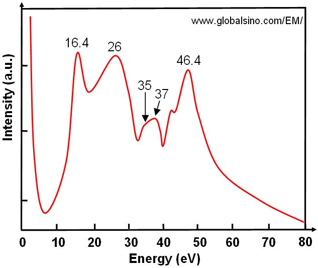
Figure 2069b. Theoretical low energy loss spectrum of EELS simulated from HfO2 film. |
The Hf4f7/2 peak at the binding energy between 16.4 and 17.0 eV (attributed to O–Hf–O bonding
states) in XPS shown in Figure 2069c indicates the stoichiometric
formation of HfO2. On the other hand, the binding energy of 29.8 eV is assigned to the 5p3/2 levels of HfO2 (not shown). Table 2069d lists the positions of the peaks of the Hf4f7/2 core-level in XPS spectra taken from different crystal structures.
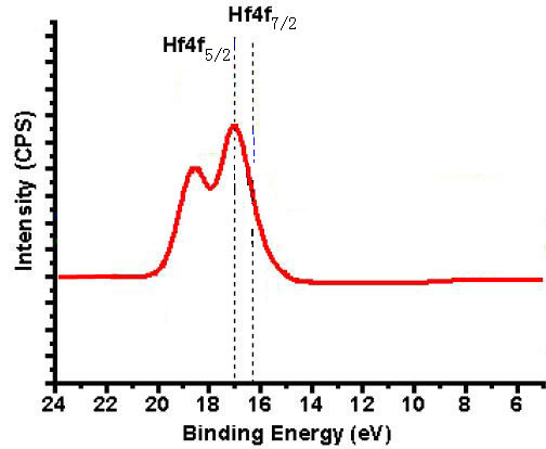
Figure 2069c. XPS of HfO2.
| Table 2069d. Positions of the peaks of the Hf 4f7/2 core-level in XPS spectra taken from different HfO2 crystal structures and films. |
| HfO2 crystal structure/film/bond |
Hf 4f7/2(eV) |
Reference |
Monoclinic + orthorhombic |
18.0 - 18.5 |
[30] |
| Monoclinic |
16.4 - 16.7 |
[35-36] |
| Cubic |
17.8 - 18.1 |
[31-34] |
| Thick films (e.g. 26.5 nm) |
16.8 |
[44] |
| Thin films (e.g. 0.6 and 5 nm) |
Very much scattered (17.06 - 18.3) |
[35-43] |
| Alumina addition |
Increase the binding energy |
[47-49] |
| Yttrium addition |
~18.1 |
[50] |
| Formation of hafnium
silicate |
Induces a shift toward higher binding
energies, e.g. 17.4-18.3 |
[45-46] |
| Hf–O–N
bond |
16.4 |
[51, 52] |
| Hf–N bond |
15.3–15.8 |
[51, 52] |
[1] Stefan Mueller, Johannes Mueller, Aarti Singh, Stefan Riedel, Jonas Sundqvist, Uwe Schroeder and Thomas Mikolajick, Incipient Ferroelectricity in Al-Doped HfO2 Thin Films, 22(11), 2412–2417, 2012.
[2] Patrick D. Lomenzo, Peng Zhao, Qanit Takmeel, Saeed Moghaddam, Toshikazu Nishida, Matthew Nelson, Chris M. Fancher, Everett D. Grimley, Xiahan Sang, James M. LeBeau and Jacob L. Jones, Ferroelectric phenomena in Si-doped HfO2 thin films with TiN and Ir electrodes, J. Vac. Sci. Technol. B 32, 03D123 (2014).
[3] Yeon Woo Yoo, Woojin Jeon, Woongkyu Lee, Cheol Hyun An, Seong Keun Kim, and Cheol Seong Hwang, Structure and Electrical Properties of Al-Doped HfO2 and ZrO2 Films Grown via Atomic Layer Deposition on Mo Electrodes, ACS Appl. Mater. Interfaces, 6 (24), 22474–22482 (DOI: 10.1021/am506525s), 2014.
[4] Shuai Chen, Zhengtang Liu, Liping Feng, Xiaoru Zhao, Photoluminescent properties of undoped and Ce-doped HfO2 thin films prepared by magnetron sputtering, Journal of Luminescence, 153, 148–151, 2014.
[5] Mei Ji, Lei Wang, Jun Du, Preparation and characterization of Gd2O3-doped HfO2 high-k gate dielectric thin films by RF
sputtering, Journal of Physics: Conference Series 152 (2009) 012005.
[6] S. Mueller, C. Adelmann, A. Singh, S. Van Elshocht, U. Schroeder,
and T. Mikolajick, Ferroelectricity in Gd-Doped HfO2 Thin Films, ECS Journal of Solid State Science and Technology, 1 (6) N123-N126 (2012).
[7] C. Adelmann, H. Tielens, D. Dewulf, A. Hardy, D. Pierreux, J. Swerts, E. Rosseel,
X. Shi, M. K. Van Bael, J. A. Kittl, and S. Van Elshocht, J. Electrochem. Soc., 157,
G105 (2010).
[8] A. Hardy, C. Adelmann, S. Van Elshocht, H. Van den Rul, M. K. Van Bael,
S. De Gendt, M. D’Olieslaeger, M. Heyns, J. A. Kittl, and J. Mullens, Appl. Surf.
Sci., 255, 7812 (2009).
[9] Martin, D., Yurchuk, E. ; Muller, S. ; Muller, J. ; Paul, J. ; Sundquist, J. ; Slesazeck, S. ; Schloesser, T. ; van Bentum, R. ; Trentzsch, M. ; Schroeder, U. ; Mikojajick, T., Downscaling ferroelectric field effect transistors by using ferroelectric Si-doped HfO2, 2012 13th International Conference on Ultimate Integration on Silicon (ULIS), 2012 (DOI:
10.1109/ULIS.2012.6193391).
[10] Gao, L., et al., Stabilization of cubic structure in Mn-doped hafnia. Ceramics International, 2012. 38(3): 2305-2311.
[11] Losovyj, Y.B., et al., The electronic structure change with Gd doping of HfO2 on silicon. Applied Physics Letters, 2007.
91(13): 3.
[12] Matovic, B., et al., Synthesis and characterization of nanometric yttrium-doped hafnia solid solutions. Journal of the
European Ceramic Society, 2012. 32(9): 1971-1976.
[13] Ortega, A., et al., Correlation between phase and optical properties of yttrium-doped hafnium oxide nanocrystalline
thin films. Optical Materials, 2013. 35(9): 1728-1734.
[14] Buha, J., et al., Solvothermal and surfactant‐free synthesis of crystalline Nb2O5, Ta2O5, HfO2, and Co‐doped HfO2
nanoparticles. Physical Chemistry Chemical Physics, 2010. 12(47): 15537‐15543.
[15] M. Yashima, H. Takahashi, K. Ohtake, T. Hirose, M. Kakihana, H. Arashi,
Y. Ikuma, Y. Suzuki, and M. Yoshimura, J. Phys. Chem. Solids 57, 289
(1996).
[16] H. Fujimori, M. Yashima, S. Sasaki, M. Kakihana, T. Mori, M. Tanaka,
and M. Yoshimura, Chem. Phys. Lett. 346, 217 (2001).
[17] E. Rauwel, C. Dubourdieu, B. Hollander, N. Rochat, F. Ducroquet, M. D.
Rossell, G. Van Tendeloo, and B. Pelissier, Appl. Phys. Lett. 89, 12902
(2006).
[18] 22C. Dubourdieu, E. Rauwel, H. Roussel, F. Ducroquet, B. Hollander, M.
Rossell, G. Van Tendeloo, S. Lhostis, and S. Rushworth, J. Vac. Sci. Technol.
A 27, 503 (2009).
[19] Elizabeth Navarro Cerón, Geonel Rodríguez Gattorno, Jose Guzmán-Mendoza, Manuel García-Hipólito, Ciro Falcony, Photoluminescence Response of HfO2:Eu3+ Obtained by Hydrothermal Route, Open Journal of Synthesis Theory and Applications, 2013, 2, 73-77.
[20] K. Tomida, K. Kita, and A. Toriumi, Extended Abstracts of the 2005
International Conference on Solid State Devices and Materials, 2005, 232.
[21] D. Fischer and A. Kersch, Appl. Phys. Lett. 82, 012908
(2008).
[22] D. Ramo, A. Shluger, and G. Bersuker, Phys. Rev. B 79,
035306 (2009).
[23] Mladen F. Trubeljia and Vladimir S. Stubican, J. Am.
Ceram. Soc. 74, 2489 (1991).
[24] Ching-Shiang Peng, Wen-Yuan Chang, Yi-Hsuan Lee, Ming-Ho Lin, Frederick Chen, and Ming-Jinn Tsai, Improvement of Resistive Switching Stability of HfO2 Films with Al Doping by Atomic Layer Deposition, Electrochemical and Solid-State Letters, 15 (4) H88-H90 (2012).
[25] Leonardo Miotti, Karen P. Bastos, Gerald Lucovsky, Cláudio Radtke and Dennis Nordlund, Ge doped HfO2 thin films investigated by x-ray absorption spectroscopy, J. Vac. Sci. Technol. A 28, 693 (2010).
[26] L. G. Wang, Y. Xiong, W. Xiao, L. Cheng, J. Du, H. Tu, and A. van de Walle, Computational investigation of the phase stability and the electronic properties for Gd-doped HfO2, Applied Physics Letters 104, 201903 (2014).
[27] Su-Shia Lin, Han-Ru Li, The optical properties of hydrophilic Hf-doped HfO2 nanoceramic films, Ceramics International, 39(7) 7677-7683, 2013.
[28] TS Böscke, J Müller, D Bräuhaus, U Schröder, U Böttger, Ferroelectricity in hafnium oxide thin films, Applied Physics Letters, 99, 102903-102903-3, 2011.
[29] Johannes Müller, Tim S Böscke, Uwe Schröder, Stefan Mueller, Dennis Bräuhaus, Ulrich Böttger, Lothar Frey, Thomas Mikolajick, Ferroelectricity in Simple Binary ZrO2 and HfO2, Nano Lett 2012 Aug 23;12(8):4318-23.
[30] 17D. R. Wilder, J. D. Buckley, D. W. Stacy, and J. K. Johnstone, Characterization
and control of the destructive crystalline transformation in
hafnium oxide, Colloques internationaux du CNRS, N° 205—Etude des
transformations cristallines à hautes temperatures, 1973.
[31] A. Weyl and D. Janke, J. Am. Ceram. Soc. 79, 2145, 1996.
[32] P. Chen, H. B. Bhandari, and T. M. Klein, Appl. Phys. Lett. 85, 1574,
2004.
[33] F. Zhu et al., Appl. Phys. Lett. 89, 173501, 2006.
[34] A. E.-J. Lim, R. T. P. Lee, X. P. Wang, W. S. Hwang, C. H. Tung, G. S.
Samudra, D.-L. Kwong, and Y.-C. Yeo, IEEE Electron Device Lett. 28,
482, 2007.
[35] J. F. Moulder, W. F. Stickle, P. E. Sobol, and K. D. Bomben, Handbook of
X-ray Photoelectron Spectroscopy, Perkin Elmer, Eden Prairie, MN,
1992.
[36] D. D. Sharma and C. N. R. Rao, J. Electron Spectrosc. Relat. Phenom.
20, 25, 1980.
[37] S. Sayan, E. Garfunkel, and S. Suzer, Appl. Phys. Lett. 80, 2135, 2002.
[38] T. P. Smirnova, L. V. Yakovkina, V. N. Kitchai, V. V. Kaichev, Yu. V.
Shubin, N. B. Morozova, and K. V. Zherikova, J. Phys. Chem. Solids 69,
685, 2008.
[39] M. Kundu, N. Miyata, T. Nabatame, T. Horikawa, M. Ichikawa, and A.
Toriumi, Appl. Phys. Lett. 82, 3442, 2003.
[40] S. Suzer, S. Sayan, M. M. Banaszak Holl, E. Garfunkel, Z. Hussain, and
N. M. Hamdan, J. Vac. Sci. Technol. A 21, 106, 2003.
[41] S. Toyoda, K. Okabayashi, H. Kumigashira, M. Oshima, K. Ono, M.
Niwa, K. Usuda, and G. L. Liu, Appl. Phys. Lett. 84, 2328, 2004.
[42] O. Renault, D. Samour, J.-F. Dalemcourt, D. Blin, F. Martin, S. Marthon,
N. T. Barrett, and P. Besson, Appl. Phys. Lett. 81, 3627, 2002.
[43] N. Barrett, O. Renault, J.-F. Dalemcourt, and F. Martin, J. Appl. Phys. 96,
6362, 2004.
[44] M.-H. Cho Y. S. Roh, C. N. Whang, K. Jeong, S. W. Nahm, D.-H. Ko, J.
H. Lee, N. I. Lee, and K. Fujihara, Appl. Phys. Lett. 81, 472, 2002.
[45] V. Cosnier, M. Olivier, G. Théret, and B. André, J. Vac. Sci. Technol. A
19, 2267, 2001.
[46] G. D. Wilk, R. M. Wallace, and J. M. Anthony, J. Appl. Phys. 87, 484, 2000.
[47] P. F. Lee, J. Y. Dai, K. H. Wong, H. L. W. Chan, and C. L. Choy, J. Appl.
Phys. 93, 3665, 2003.
[48] M.-H. Cho et al., Surf. Sci. 554, L75, 2004.
[49] H. Grampeix et al., ECS Trans. 11, 213, 2007.
[50] Z. K. Yang et al., Appl. Phys. Lett. 91, 202909, 2007.
[51] C. S. Kang, H.-J. Cho, K. Onishi, R. Nieth, R. Choi, S. Gopalan, S.
Krishnan, J. H. Han, and Jac C. Lee, Appl. Phys. Lett. 81, 2593, 2002.
[52] M. Koyama, A. Kaneko, T. Ino, M. Koike, Y. Kamata, R. Iijima, Y.
Kamimuta, A. Takashima, M. Suzuki, C. Hongo, S. Inumiya, M. Takayanagi,
and A. Nishiyama, Tech. Dig. - Int. Electron Devices Meet.
849, 2002.
[53] Uwe Schroeder, Claudia Richter, Min Hyuk Park, Tony Schenk, Milan Pešić, Michael Hoffmann, Franz P. G. Fengler, Darius Pohl, Bernd Rellinghaus, Chuanzhen Zhou, Ching-Chang Chung, Jacob L. Jones, and Thomas Mikolajick, Lanthanum-Doped Hafnium Oxide: A Robust Ferroelectric Material, Inorg. Chem. 2018, 57, 5, 2752-2765.
[54] Michal Mazur, Danuta Kaczmarek, Jaroslaw Domaradzki, Damian Wojcieszak and Agata Poniedzialek, Influence of Material Composition on Structural and Optical Properties of HfO2-TiO2 Mixed Oxide Coatings, Coatings 2016, 6, 13.
|
