| Table 3025a. Fm-3m (225) space group.
Name in the International Tables for Crystallography |
Fm-3m |
|
F |
|
225 |
|
m-3m |
Crystal system |
Cubic |
|
m-3m |
Pearson symbol |
cF12, cF8, etc. |
|
192 |
Structure type |
NaCl-type structure |
|
1, √3, √4, √8, √11, √12, √16, √19, √20, √24, √27, ... |
Symmetry (atomic coordinates) |
X, Y, Z; -X, -Y, Z; -X, Y, -Z; X, -Y, -Z; Z, X, Y; Z, -X, -Y; -Z, -X, Y; -Z, X, -Y; Y, Z, X; -Y, Z, -X; Y, -Z, -X; -Y, -Z, X; Y, X, -Z; -Y, -X, -Z; Y, -X, Z; -Y, X, Z; X, Z, -Y; -X, Z, Y; -X, -Z, -Y; X, -Z, Y; Z, Y, -X; Z, -Y, X; -Z, Y, X; -Z, -Y, -X; -X, -Y, -Z; X, Y, -Z; X, -Y, Z; -X, Y, Z; -Z, -X, -Y; -Z, X, Y; Z, X, -Y; Z, -X, Y; -Y, -Z, -X; Y, -Z, X; -Y, Z, X; Y, Z, -X; -Y, -X, Z; Y, X, Z; -Y, X, -Z; Y, -X, -Z; -X, -Z, Y; X, -Z, -Y; X, Z, Y; -X, Z, -Y; -Z, -Y, X; -Z, Y, -X; Z, -Y, -X; Z, Y, X; X, 1/2+Y, 1/2+Z; -X, 1/2-Y, 1/2+Z; -X, 1/2+Y, 1/2-Z; X, 1/2-Y, 1/2-Z; Z, 1/2+X, 1/2+Y; Z, 1/2-X, 1/2-Y; -Z, 1/2-X, 1/2+Y; -Z, 1/2+X, 1/2-Y; Y, 1/2+Z, 1/2+X; -Y, 1/2+Z, 1/2-X; Y, 1/2-Z, 1/2-X; -Y, 1/2-Z, 1/2+X; Y, 1/2+X, 1/2-Z; -Y, 1/2-X, 1/2-Z; Y, 1/2-X, 1/2+Z; -Y, 1/2+X, 1/2+Z; X, 1/2+Z, 1/2-Y; -X, 1/2+Z, 1/2+Y; -X, 1/2-Z, 1/2-Y; X, 1/2-Z, 1/2+Y; Z, 1/2+Y, 1/2-X; Z, 1/2-Y, 1/2+X; -Z, 1/2+Y, 1/2+X; -Z, 1/2-Y, 1/2-X; -X, 1/2-Y, 1/2-Z |
Crystal examples |
CaF2: Ca at (0, 0, 0) and
F at (1/4, 1/4, 1/4).
NaCl: Na at (0, 0, 0) and
Cl at (1/2, 1/2, 1/2).
TiN: Ti (1a) at (0, 0, 0), and N (1b) at (0, 0.5, 0)
Crystals in Figure 3025b. |
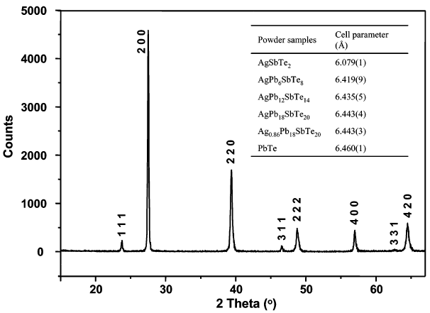
Figure 3025a. Typical example of X-ray powder diffraction patterns obtained from Fm-3m single-phase structures (AgPb6SbTe8, AgPb12SbTe14, AgPb18SbTe20, Ag0.86Pb18SbTe20, AgSbTe2, and
PbTe compounds). [1] Note that we can index diffraction patterns starting from comparing experimental d-spacings and theoretical calculations obtained from known lattice parameters, for instance, use the excel file for crystals with Fm-3m space group.
|
|
|
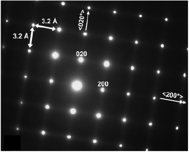
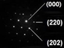
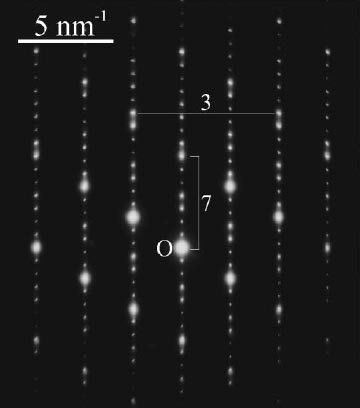
[0 0 1] Ag0.95Pb15SbTe17.
(a = 0.64 nm) [1] |
|
|
|
|
|
[0 0 1] Ge2Bi2Te5. [3] |
4mm net symmetry in ZOLZ [001] zone-axis of Zr41Ti14Cu12.5Ni10Be22.5 ( a = 1.185 nm) [4] |
|
|
|
|
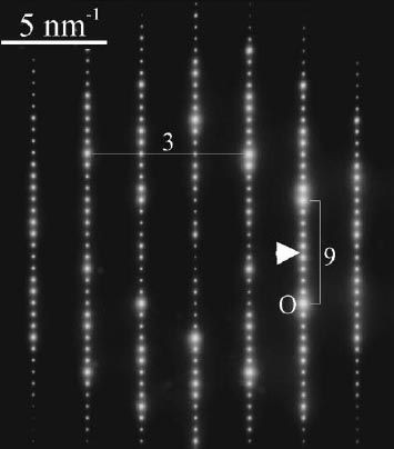
[0 1 1] Ag0.95Pb15SbTe17.
(a = 0.64 nm) [1] |
[1 1 0] Ge2Sb2Te5 (GST). [2] |
[1 1 0] Ge2Bi2Te5. [3] |
|
|
|
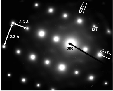
[-1 1 1] Ge2Sb2Te5 (GST). [2] |
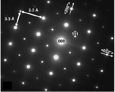
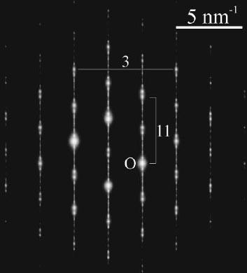
[1 1 1] Ag0.95Pb15SbTe17.
(a = 0.64 nm) [1] |
|
|
|
|
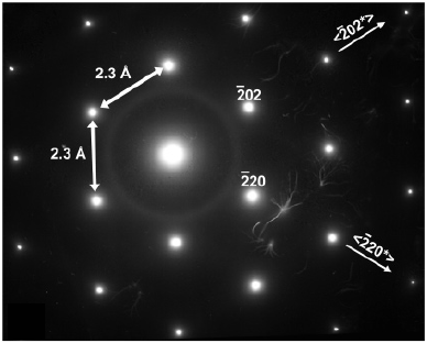
[-1 1 2] Ag0.95Pb15SbTe17.
(a = 0.64 nm) [1] |
|
|
|
|
|
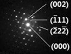
Figure 3025b. Examples of indexed electron diffraction (or FFT) patterns of Fm-3m (225) cubic crystals.
[1] Eric Quarez, Kuei-Fang Hsu, Robert Pcionek, N. Frangis, E. K. Polychroniadis, and Mercouri G. Kanatzidis, Nanostructuring, Compositional Fluctuations, and Atomic Ordering in the Thermoelectric Materials AgPbmSbTe2+m. The Myth of Solid Solutions, J. AM. CHEM. SOC. 127, 9177-9190, 2005.
[2] J.J. Zhao, F.R. Liu, X.X. Han, Z. Zhu, X. Lin, F. Liu, N.X. Sun, Transmission electron microscopy study of amorphous Ge2Sb2Te5films induced by an ultraviolet single-pulse laser, Applied Surface Science 311 (2014) 83–88.
[3] Chang Woo Sun, A Transmission Electron Microscopy Study on the Microstructural Properties of Te-based Chalcogenide Thin Films, Doctoral Thesis, 2010.
[4] Q. Wei, N. Wanderka, P. Schubert-Bischoff, and M-P. Macht, S. Friedrich, Crystallization phases of the Zr41Ti14Cu12.5Ni10Be22.5 alloy after slow solidification, J. Mater. Res., 15 (8) 1729, (2000).
|

![A [001] diffraction pattern obtained from Ag0.95Pb15SbTe17 (space group: Fm-3m)](image2/3024a.gif)
![Electron diffraction pattern obtained from [001] Ag0.95Pb15SbTe17 (space group: Fm-3m) with splitting of electron reflections](http://www.globalsino.com/EM/image2/2023a.gif)
![[0 0 1] Ge2Bi2Te5](image2/3039d.jpg)
![4mm net symmetry in ZOLZ in [001] zone-axis of Zr41Ti14Cu12.5Ni10Be22.5](http://www.globalsino.com/EM/image2/3001.gif)
![[1 1 0] Ge2Bi2Te5](image2/3039e.jpg)