
Chapter/Index: Introduction | A | B | C | D | E | F | G | H | I | J | K | L | M | N | O | P | Q | R | S | T | U | V | W | X | Y | Z | Appendix
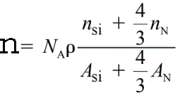
| The EELS of the low-energy loss region less than 50 eV is particularly called valence electron energy loss spectroscopy (VEELS) and mainly reflects the excitation of valence band electrons, such as interband transition (single excitation) and plasmon excitation (collective excitation). VEELS can be applied to analyze, for instance, local electronic and optical properties of materials [1] in nanoscale with STEM [2–7]. The STEM-VEELS method provides various advantages over conventional optical spectroscopy, for instance, it can measure a wider energy (wavelength) range and local electronic and optical properties from a small volume in a nano-region. The difficulty of STEM-VEELS application is that it is hard to fit a zero-loss tail, to extract ELF (energy loss function) attributable to the large zero-loss tail and to interpret the collective excitation such as plasmon, etc. Both the valence electron peaks and the ionization edges represent a fine structure that reflects the crystallographic or energy band structure of the specimen.For instance, the density (n) of valence electrons in Si3N4 is given by, ELNES mapping is enabled by the fact that chemical bonding and short-range order in the environment of a specific chemical element induce a chemical shift of the energy-loss edge in the range between 0.1 and 8 eV and modifies the near-edge fine structure (ELNES) of the electron energy-loss spectrum. Therefore this method can differentiate between compounds of the same binary or multi-component system but with different bonding and valency. In contrast to core electrons, valence electrons have a very large scattering cross section, providing higher spatial resolution because smaller spot sizes can be used and induces less sample damage and smaller exposure times can be applied. The signatures of the valence electrons can be considered as a finger print of compounds, not of the elements. However, a disadvantage is that it is still very difficult to predict theoretically the position and the shape of plasmons for a given compound so that VEELS is applicable only when there are reference spectra. For instance, VEELS provides the information on the dielectric response of material valence electrons, including both the single electron interband excitations from the valence band (VB) to the conduction band (CB) and the collective oscillations of valence electrons (i.e., plasmon excitations).[1] VEELS measurements can be acquired with a parallel electron energy-loss spectrometer (PEELS) fitted to a STEM operating at 200 keV and a dedicated STEM operating at 100 keV, offering spatial resolution superior to the conventional optical means. The sp2 bonded solids have both σ/σ* and π/π* states available to the electrons, while for sp3 bonded solids only the σ/ σ* states present. For the diamond and graphite, electron transitions to these states generate many of the characteristic features in EEL spectra. For instance, in core loss spectra from diamond, the excitation of the 1s electrons to the σ* states generates the carbon k edge peak. For graphite, the transitions of the inner shell electrons into unoccupied π* states give a peak prior to the edge onset. In the valence band, valence electron transitions into the π* states also produce a peak at around 6 eV. Table 4361 lists an example of experimental settings for VEELS measurements. Table 4361. Example of experimental settings for VEELS measurements.
[1] R. F. Egerton, Electron Energy Loss Spectroscopy in the Electron Microscope
(Plenum, New York, 1996).
|
 ------------------------- [4361]