
Chapter/Index: Introduction | A | B | C | D | E | F | G | H | I | J | K | L | M | N | O | P | Q | R | S | T | U | V | W | X | Y | Z | Appendix
| The EELS recorded up to a few tens of electron volts is sometimes called the low-loss region. In general, the term “low-loss’’ is used to describe the energy-loss of electrons in the range up to ~50 eV. The low-loss region is dominated by collective excitations (plasmons) [1] or by inter- or intra-band transitions. Typical values of the plasmon energies of materials are between 5 eV and 30 eV. The plasmon peaks are thus in the low energy loss region. Even though this signal is intensive, the interpretation is difficult because the excitation probability depends on both valence and conduction band states. Actually, the EELS in the low-energy loss region less than 50 eV is particularly called valence electron energy loss spectroscopy (VEELS). This low loss region mainly reflects: Both i and ii) above determine the optical properties of materials. VEELS can be applied to analyze, for instance, local electronic and optical properties of materials [2] in nanoscale with STEM [3–8]. The STEM-VEELS method provides various advantages over conventional optical spectroscopy, for instance, it can measure a wider energy (wavelength) range and local electronic and optical properties from a small volume in a nano-region. The difficulty of STEM-VEELS application is that it is hard to fit a zero-loss tail, to extract ELF (energy loss function) attributable to the large zero-loss tail and to interpret the collective excitation such as plasmon, etc. On the other hand, zero-loss can be originally from interaction between incident electron beam and atomic nuclei and also arise from inelastic scattering by conduction or valence electrons. The EEL spectrum can be described in a dielectric formulation [2] by, where, Based on Equation 4776 and a Kramers–Kronig analysis, the complex dielectric function ε = ε1 + iε2 can be obtained from the low-loss EEL spectrum. In general, the requirements of TEM specimen thickness for EELS and EFTEM measurements are:
[1] Egerton R. F., Electron Energy Loss Spectroscopy in the Electron Microscope. New York: Plenum, 1986.
|
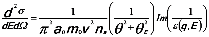 -------- [4776]