Chapter/Index: Introduction | A | B | C | D | E | F | G | H | I | J | K | L | M | N | O | P | Q | R | S | T | U | V | W | X | Y | Z | Appendix
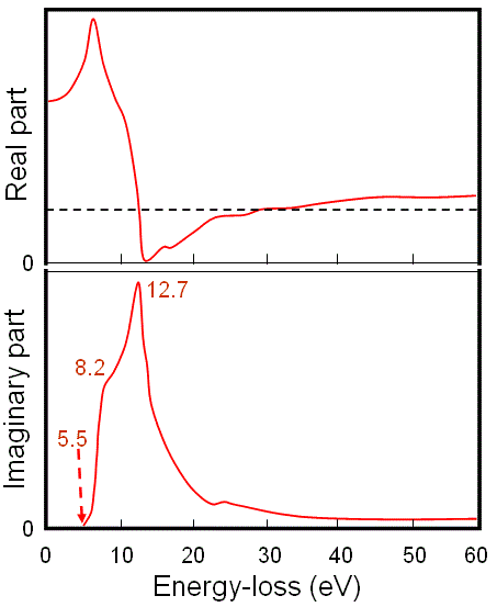
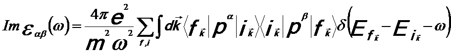
| The EELS of the low-energy loss region less than 50 eV is particularly called valence electron energy loss spectroscopy (VEELS) and mainly reflects the excitation of valence band electrons, such as interband transition (single excitation) and plasmon excitation (collective excitation). VEELS can be applied to analyze, for instance, local electronic and optical properties of materials [7] in nanoscale with STEM [8–13]. The STEM-VEELS method provides various advantages over conventional optical spectroscopy, for instance, it can measure a wider energy (wavelength) range and local electronic and optical properties from a small volume in a nano-region. The difficulty of STEM-VEELS application is that it is hard to fit a zero-loss tail, to extract ELF (energy loss function) attributable to the large zero-loss tail and to interpret the collective excitation such as plasmon, etc. It was suggested [19] that the probabilities of the ELF for surface and bulk plasmons are given by Im[−1/(ε + 1)] and Im[−1/(ε)], respectively. The dielectric function describes the response of the material to a time-dependent electromagnetic field. Since the single and collective excitations induced by the interaction of incident electrons with materials are related to the real (ε1) and imaginary (ε2) parts of the dielectric function ε(ω) in different ways [15], the ε(ω) is used to describe and distinguish the single and collective excitations [1]. If the material is anisotropic, the microscopic dielectric function can be a tensor εαβ, given by, [6] where, The energies of collective oscillations can be extracted from the dielectric function by calculating the energy loss functions for the surface and bulk solid, which are given by Im(-1/ε) and Im[-1/(1+ε)], respectively. According to Drude model [2,3], the energy loss function for a bulk plasmon can be given by, where, That means the transfer of the energy E (or momentum q) of the incident electrons to the solid electrons is related to the complex dielectric function of the solid ε = ε1 + iε2 through its imaginary part Im[−1/ε], while the intensity damping, due to the propagation in the dielectric medium, is proportional to ε2. Figure 4360a presents the ELF and ε1 and ε2 as a function of energy loss. The arrows show the plasmon peaks and the corresponding ε1 around their values close to 0. The three plasmon peaks are at around 12 eV, 18 eV, and 24 eV.
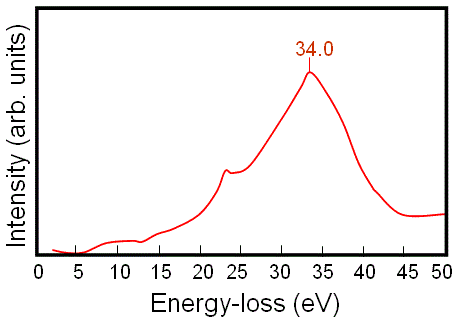
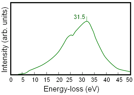
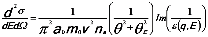
Figure 4360a. The ELF and ε1 and ε2 as a function of energy loss. [14] The energy loss function is the relationship between the dielectric response of electrons and the EELS spectrum. Therefore, the EEL spectrum can be described in a dielectric formulation [5] by, where, An optical absorption method can directly provide the imaginary part of the dielectric function, ε2, associated with a single electron excitation of an interband transition, while EELS cannot directly give ε2. Based on Equation 4360c and a Kramers–Kronig analysis, the complex dielectric function ε = ε1 + iε2 can still be obtained from the low-loss EEL spectrum.The plasmon signal in EELS can be applied to extract dielectric function [4], valence electron densities, and, in some cases, the phases presented in alloys. Therefore, because of the relationship indicated in Equation 4360b, the real (ε1) and the imaginary (ε2) parts of the dielectric function can be extracted by a Kramers-Kronig analysis. The experimental single scattering distribution S(E) can be given by, [2, 16-18] In both Equations 4360c and 4360d, for small q, ε(q,E) varies very slowly with q and thus it can be replaced by ε(E). Figure 4360b shows the EEL spectra of plasmon region (zero-peak is not shown) for crystalline and amorphous diamond. The loss function (Im[-l/ε]) can then be obtained by removing contribution from multiple scattering using the Fourier-log deconvolution method.
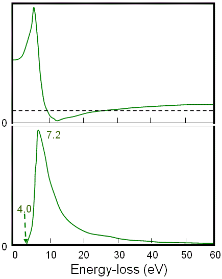
Figure 4360b. EEL spectra of plasmon region for (a) crystalline and (b) amorphous diamond. Based on the obtained loss function, the real part (ε1), and the imaginary part (ε2) of the dielectric function for the crystalline and the amorphous diamond are extracted using Kramers-Kronig analysis as shown in Figure 4360c. Table 4360 lists the onset energy (indicating the band gap energy) and the peaks in the imaginary spectrum obtained from Figure 4360c and the original interband transitions. In many cases, the broad maxima in ε2, e.g. with energies higher than 10 eV, represent widely distributed oscillator strengths. That is, the peaks in ε2 correspond to some interband transitions. The real part ε1 of the dielectric function decreases to ~0, indicating a resonance [20]. The resonance in insulators depends on the collective oscillation of the electrons in the valence band. In metals, the resonance depends on the collective oscillations of the free electron gas near the Fermi surface excited by the long-range Coulomb interactions. Furthermore, the resonance of free electron gas in metals is much stronger than that of bound electrons in the valence band of insulators [21].
Figure 4360c. Real part (ε1), and the imaginary part (ε2) of the dielectric function for (a) crystalline and (b) amorphous diamond. Table 4360. Onset energies (band gap energies), peaks in the imaginary spectrum in Figure 4360c and the original interband transitions.
As discussed above, the energy loss spectrum cannot be directly associated with interband transitions because its peak positions at low energy losses are strongly affected by the volume plasmon and the positions of other excitations. The imaginary part of the dielectric function, however, can be associated with interband transitions. The common procedure of obtaining the real and imaginary parts of the dielectric function is summarized below: Note that if the EELS energy resolution is poor, then the data at low energy range will be not reliable, for instance, the data below 3 eV are not reliable with an common energy resolution of 1.3 eV. If the SSD (single-scatter distribution) is known then optical techniques such as Kramers–Kronig analysis can be applied to determine the dielectric function, reflectivity, absorption, etc. [7]
[1] Ritchie R.H. and Howie A., Phil. Mag. 36 (1977) 463.
|
 -------- [4360a]
 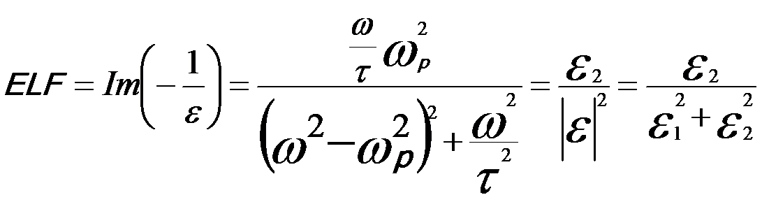 ---------------------- [4360b]
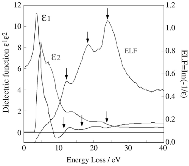
 -------- [4360c]
 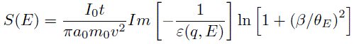 -------- [4360d]