=================================================================================
The loosely bound electrons in the valence and
conduction bands can oscillate collectively around the quasi-stationer set of nuclei, producing
oscillating polarization that can be described by a quasi-particle, called plasmon. As listed in Table 3417a, the bulk plasmon is a collective oscillation of the
loosely bound electrons. In EEL spectrum (EELS), the peak next to the zero loss peak is caused by excitation of surface and/or bulk plasmons. The energy region of the EEL spectrum up to the energy loss of ~50 eV is dominated by the collective excitations of valence electrons (plasmon) and by interband transitions. The plasmon peak is the second most dominate feature after the zero-loss peak. Typical values of the plasmon energies of materials are between 5 eV and 30 eV and it can vary due to some mechanisms (refer to Origin of Change of Plasmon Energy). The plasmon peaks are thus in the low energy loss region. The plasmons can provide information about the dielectric function [1], valence electron densities, and, in some cases, the phases presented in alloys.
| Table 3417a. Main physical mechanisms which the energy and intensity of the plasmon peak represents. |
Materials
|
Main mechanisms |
General |
Oscillation of loosely bound electrons (conduction and valence-band electrons) |
Metals |
Excitation of free-electron gas (electrons in conduction-band) |
Semiconductor |
Resonance of valence electrons |
Plasmon consists of longitudinal wave-like oscillations of weakly bonded electrons. The collective oscillations are rapidly damped with a typical lifetime of ~10-15 seconds and thus are localized to <10 nm. For many materials the plasmon energy, based on free-electron theory (Drude model [2]), Eplasmon, is proportional to the square root of the density (n) of valence electrons (approximately equal to free-electron density):
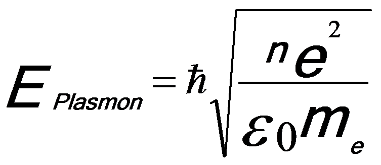 ------------------------- [3417a] ------------------------- [3417a]
= ħω(q) ------------------------- [3417b]
where,
ħ -- The reduced Planck constant.
n -- The density of valence electrons.
e -- The charge of the electron.
me -- The effective mass of the electron.
ε0 -- The permittivity of vacuum (or called the dielectric constant of free space).
For instance, the density (n) of valence electrons in Si3N4 is given by,
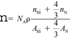 ------------------------- [3417c] ------------------------- [3417c]
where,
ρ -- The Si3N4 atomic density (3.0 g/cm3),
NA -- The Avogadro number,
ASi
and AN -- The atomic weights of silicon and nitrogen, respectively,
nSi and nN -- The numbers of valence electrons per silicon and per
nitrogen atom taking part in the plasmon oscillation, respectively. nSi= 4 and nN = 3~5.
Since the density of valance electrons in different materials such as Si3N4, SiO2, and Si are different, the bulk plasmon energies are also different in these materials.
The plasmon
energy can be changed by:
i) the density of valence electrons in insulators and semiconductors as shown in Equation 3417a.
ii) the density of loosely bound states in metals. For instance, when pure aluminum (Al) is alloyed with another
element, the density of loosely bound states invariably
decreases, with a resulting change in the plasmon
energy.
Table 3417b shows the properties of surface and bulk plasmons. For instance, at the energy of 2000 eV of an incident electron beam, the Si 2p electrons with a binding energy of about 100 eV will have a kinetic energy of 1900 eV, while at the energy of 150 eV, the same Si 2p electrons will have a kinetic energy of about 50 eV. Therefore, bulk plasmon can be investigated with high energy EELS and plasmon in a thin surface layer can be studied with low excitation energy.
Table 3417b. Surface and bulk plasmons.
|
Comments |
Surface plasmon |
Transverse waves, half the energy of
bulk plasmons |
Bulk plasmon |
Longitudinal waves |
For thick TEM specimens, a significant portion of the electron beam has undergone inelastic scattering many times. In each scattering event, the incident electrons lose 16.7 eV [page4623] so that those electrons that have
scattered twice present an energy peak at 2 x 16.7 = 33.4 eV, those that scattered 3 times add a peak at 3x16.7=50.1 eV, and those that scattered 4 times at 4x16.7 = 66.8 eV, etc (see Figure 3417a).
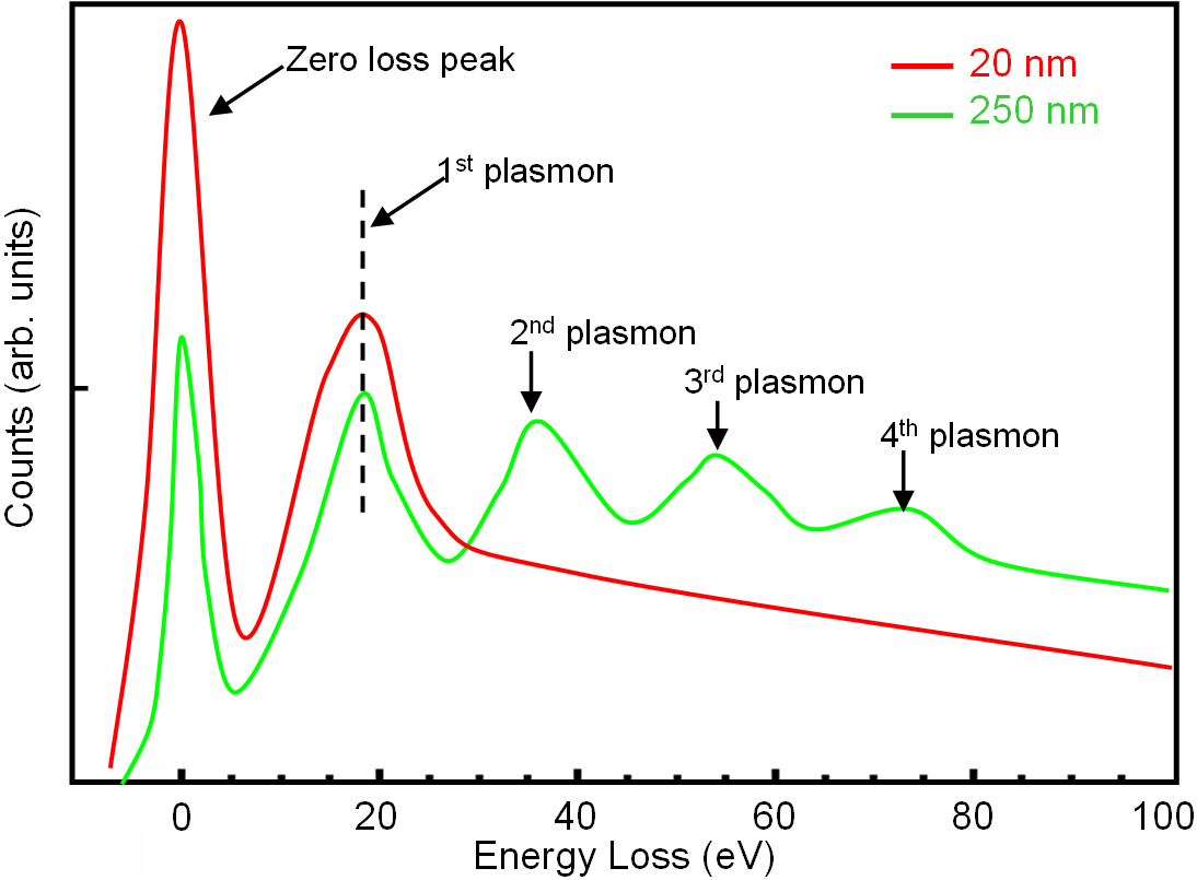
Figure 3417a. Low energy loss of silicon (Si) TEM film with specimen thickness of 20 and 250 nm. |
The plasmon energy loss can experimentally provide indirect semi-quantitative information because the free-electron density n changes with the chemistry or bonding state of the TEM specimen. The empirical plasmon peak position (Ep) can be given by,
Ep = Ep(0) ± C(dEp/dC) ------------------------------------ [3417c]
where,
Ep(0) -- The plasmon energy loss for the pure component (See the table on page4623).
C -- The composition.
Therefore, once Ep is obtained from EELS measurement, then C can be evaluated. For instance, as shown in Figure 3417b, empirical sp2/sp3 ratios in amorphous carbons were evaluated based on Equation 3417c and the relative intensity of k-edge 1s to π* transition [4-8].
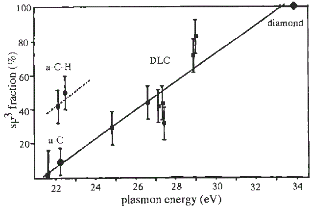
Figure 3417b. Fraction of sp3 bonding as a function of the bulk plasmon energy. [4]
The Drude-Lorentz model presents the maximum intensity of the plasmon energy loss peak, given by, [3]
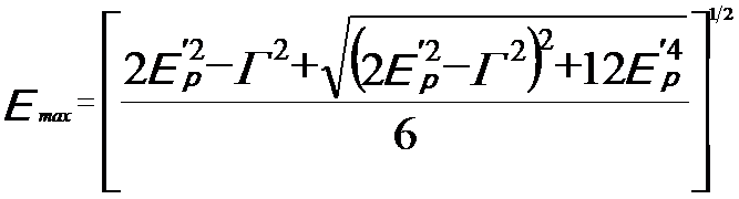 ---------- [3417d] ---------- [3417d]
where,
Γ -- A constant describing the damping of the oscillation (which is full width at half maximum (FWHM) of the plasmon energy
loss peak)
And, 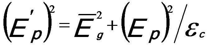 ------------------------ [3417e] ------------------------ [3417e]
where,
 -- Energy of single damped harmonic
oscillator; -- Energy of single damped harmonic
oscillator;
εc -- Dielectric constant.
The dispersion relation of bulk plasmon for small wave-vectors q is given by,
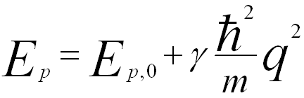 -------------------------- [3417f] -------------------------- [3417f]
where,
EP,0 -- The plasmon energy at q = 0.
γ -- An experimental coefficient.
Note that Table 4623 lists bulk plasmon energies, full-width-at-half-maximum of bulk plasmon energies, bulk plasmon mean free path, and inelastic mean free path of some common elements and compounds, as well as their crystal structure.
The interpretation of the features of low-loss regions in EELS from free-electron metals is fairly straightforward because the signals arise mainly from bulk and surface plasmon excitations and the energies of the peaks from bulk (Ebulk) and surface (Esurface) plasmon excitations have the simple relationship given by,
Ebulk = √2Esurface -------------------------- [3417g]
For thick TEM specimens, e.g. ≥80 nm for Si, the surface-plasmon effects becomes negligible, while the beam spreading becomes significant because more electrons suffer inelastic collision in larger scattering angles. In this case, more electrons scatter outside the finite collection aperture.
On the other hand, the interpretation of the features of the low-loss regions from transition metals is more difficult because of some factors. In transition metals, both plasmon losses and interband transitions induce energy loss and the plamon losses generally do not occur at the energies theoretically predicted by free-electron model. Different from the case presented in Equation 3417g for free-electron metals, there is no simple relationship between the bulk and surface plasmon loss energies for a transition metal due to too much dependence on the band structure. Moreover, some electrons in certain d-bands may not be able to participate in collective plamon oscillations.
Note that the mean-free-path is also slightly dependent on the electron optical conditions of the microscopes, such as objective and collection aperture sizes. However, in most EELS measurements, this dependence is negligible.
Page3375 lists the behaviors and properties of various inelastic electron scatterings in electron interaction with materials, including inter- and intra-band transitions, inner shell ionization, phonon excitation and plasmon excitation.
[1] Buechner, U. (1975) The dielectric function of mica and quartz determined by electron energy losses, Journal of Physics C: Solid State Physics,
8, 2781-2787.
[2] P. Drude, Phys. Z. 14, 161 (1900).
[3] A. M. Sánchez, R. Beanland, M. H. Gass, A. J. Papworth, P. J. Goodhew,
and M. Hopkinson, Phys. Rev. B 72, 075339 (2005).
[4] P.J. Fallon and L.M. Brown, Analysis of chemical-vapour-deposited diamond grain boundaries
using transmission electron microscopy and parallel electron energy loss spectroscopy
in a scanning transmission electron microscope. Diamond and Relat. Mater., 2: 1004-101 1,
1993.
[5] G.M. Pharr et al., Hardness, elastic modulus, and structure of very hard carbon films produced
by cathodic-arc deposition with substrate pulsed biasing. Appl. Phys. Lett., 68:
779-781,1996.
[6] V.I. Merkulov,D.H.Lowndes,G.E. Jellison,A.A. PuretzkyandD.B. Geohegan, Structure
and optical properties of amorphous diamond films prepared by ArF laser ablation as a
function of carbon ion kinetic energy. Appl. Phys. Lett., 73: 2591-2593,1998.
[7] S.D. Berger, D.R. McKenzie and P.J. Martin, EELS analysis of vacuum arc-deposited diamond-
like films. Phil. Mag. Lett., 57: 285-290,1988.
[8] S. Ravi et al., Nanocrystallites in tetrahedral amorphous carbon films. Appl. Phys. Lett., 69:
491493,1996.
|