Chapter/Index: Introduction | A | B | C | D | E | F | G | H | I | J | K | L | M | N | O | P | Q | R | S | T | U | V | W | X | Y | Z | Appendix
| Titanium nitride films exhibit an outstanding combination of electrical, chemical, physical, tribological, and mechanical properties, such as a high degree of electrical conductivity, resistance to atomic diffusion within its surrounding materials, chemical stability, chemical inertness, biocompatibility, high thermal conductivity, an immunity to wear and corrosion, and hardness. Titanium nitride can exist either as Ti2N or stoichiometric TiN. Thin films of TiN can be deposited by a various physical (PVD) and chemical (CVD) vapor deposition methods including evaporation, ion plating and sputtering [1, 2 – 4]. The TiN material shows a sodium chloride (NaC1) lattice, with Ti atoms in a fcc arrangement and N atoms partly occupying the octahedral interstices, normally at very small grain sizes. In the lattice structure, Ti sites are completely filled and vacancies exist only on the N sites. The properties of the thin films, such as preferred orientation of lattice plane and electrical resistance are highly dependent on total gas pressure, partial pressures of reactive gases, deposition rate, temperature and substrate material [5 – 8]. The lattice parameter (a) of TiN is ~0.435 nm, while the lattice parameters (a and c) of Ti2N are ~0.495 and ~0.303 nm, respectively. In general, the lattice parameter of non-stoichiometric compound, TiNx, can be given by, aTiNx = 4.1925 + 0.0467 x (Å) --------------------------- [2323] Here, 0.605 < x < 0.999. In IC (integrated circuits) applications, as a barrier layer it was confirmed that titanium nitride is superior to the Ti-W barrier metal and stoichiometric TiN exhibits low electrical resistivity (50-100 Ω-cm). Therefore, patterned TiN is a good material for microelectrode arrays [1]. Table 2323a. Metallization selections in ICs.
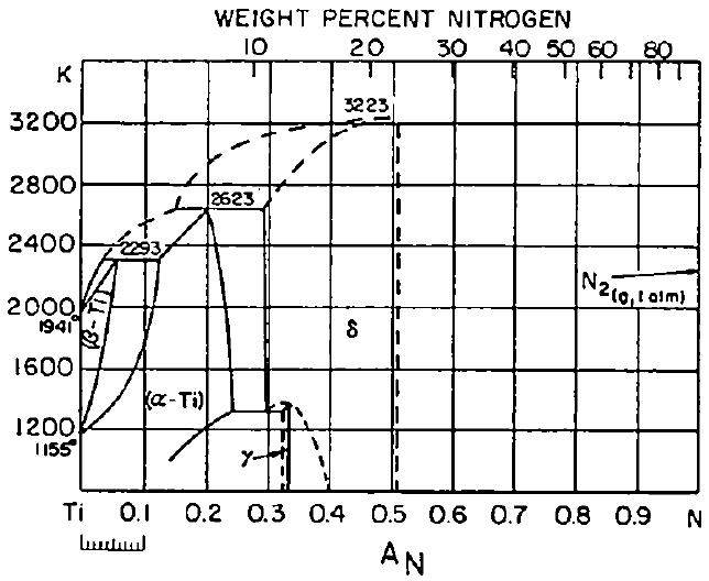
Figure 2323a shows the phase diagram of the Ti-N system.
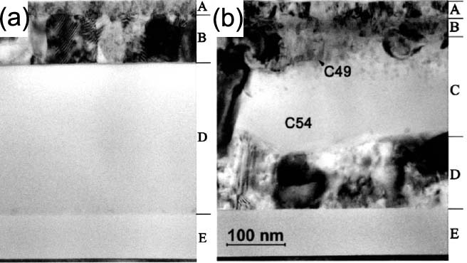
Figure 2323a. The phase diagram of the Ti-N system. AN: atomic fraction of nitrogen. [9] The TEM images in Figure 2323b shows the stacking structures before and after annealing at 900 K. The layers A, B, C, D, and E are capped TiN, deposited Ti, TiSi2, amorphous Si (for (a)) or polycrystalline Si (for (b)), and SiO2, respectively. The as-deposited TiN film has a columnar texture and is preferentially oriented with (111) planes parallel to the surface. After annealing, a TiSi2 layer with mixed C49 (close to the TiN layer) and C54 (close to the polycrystalline Si layer) phases is formed.
Figure 2323b. TEM images of the stacking structures before (a) and after (b) annealing at 900 K.
Adapted from [11]
Figure 2323c shows the [100] electron diffraction pattern and intensity distribution in the reciprocal lattice of TiN0.61.
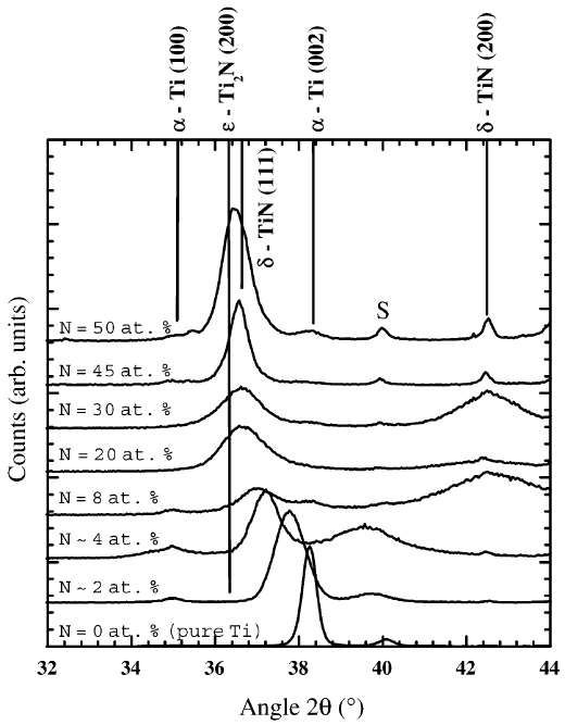
Figure 2323c. The [100] electron diffraction pattern and intensity distribution in the reciprocal lattice of TiN0.61. The large circles in (b) show the fundamental reflexions, while the small circles in (b) show the superstructure reflexions. Adapted from [9] Figure 2323d shows the shift of the XRD lines as a consequence of the progressive increase of N interstitials in octahedral α-Ti sites, which causes lattice distortion.
Figure 2323d. Evolution of the XRD patterns of the TiNx films as a function of nitrogen
contents. S corresponds to the diffraction lines of the substrate. [10] Figure 2323e shows the electric resistivity, ρ, and the hardness and Young’s modulus of TiNx films as a function of nitrogen content.
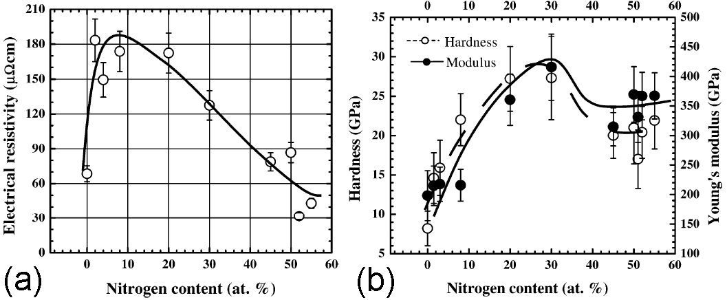
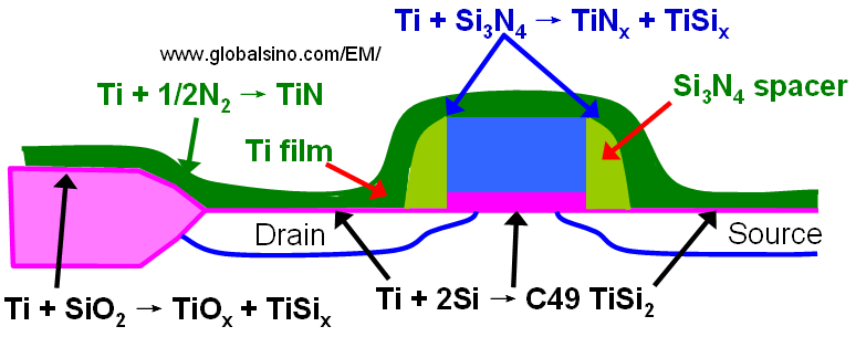
Figure 2323e. The electric resistivity, ρ, (a) and hardness and Young’s modulus (b) TiN layers have been used both as diffusion barriers and as glue layers for poorly adhering materials in the semiconductor industry. Figure 2323f shows several chemical reactions occurring during annealing of a transistor structure coated with Ti to form a low resistive TiSi2 layer at the source, gate, and drain. When silicon and titanium are reacted, Ti and Si can diffuse laterally over the isolation regions and form thin filaments of TiSix that can electronically connect a gate electrode and source/drain regions and can cause failure of the device. This phenomenon is called "bridging". On the other hand, those by-products (TiSix, TiOx, and TiN) form over the isolation regions and cannot easily be etched in conventional salicide etching solutions. The use of a nitrogen atmosphere during thermal annealing is essential in preventing this failure mechanism [12] because nitrogen quickly diffuses into the grain boundaries and significantly suppresses any long-range silicon diffusion in the titanium layer. Furthermore, to avoid the by-product formation, the annealing temperature cannot be too high.
Table 2323b. Example of properties of TiNx films.
Table 2323c. Characteristics of TixNy crystals.
Table 2323d. Other characteristics of TixNymaterials.
In IC applications, a TiN capping layer is normally used to reduce an unwanted reaction of cobalt and silicon with oxygen from air and to retard the reaction between cobalt and silicon, resulting in a high quality polycrystalline cobalt disilicide. [14]
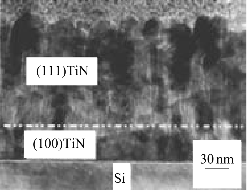
Figure 2323g. Change of TiN
orientation with thickness. [15]
[1] L. A. Cyster, D. M. Grant, K. G. Parker, T. L. Parker,
Biomol.Eng. 2002, 19, 171.
|
![[100] electron diffraction pattern and intensity distribution in the reciprocal lattice of TiN0.61](image1/2323b.jpg)