|
This book (Practical Electron Microscopy and Database) is a reference for TEM and SEM students, operators, engineers, technicians, managers, and researchers.
|
=================================================================================
SiO2 has many advantages. For instance, SiO2 is amorphous, has very few electronic defects and forms an excellent interface with Si (silicon) substrates. It can be etched and patterned to a nanometre scale.
The people now believe that the scaling limit to Moore’s law is lithography because of the need for shorter wavelengths of light to pattern the smaller feature sizes. Therefore, materials are now a key constraint in silicon technology. For example, the current density of conductors in ICs can be increased by using copper instead of aluminium. The RC time delays can be minimized using materials with lower dielectric constants instead of SiO2. Leakage in MOS structures can be minimized using materials, with high dielectric constants, between the gate and the silicon channel in FET in stead of SiO2.
Due to the continuous scaling of CMOS, the thickness of the SiO2 layer used as the gate dielectric is so thin (under 1.4 nm) that the gate leakage current due to the direct tunnelling of electrons through the SiO2 layer becomes too high (exceeding the maximum tolerable gate leakage current 1 Acm−2 at 1V) as shown in Figure 2915, therefore, the power dissipation dramatically increases to unacceptable values [1–6]. On the other hand, the reliability of the SiO2 films against electrical breakdown declines in the thin films.
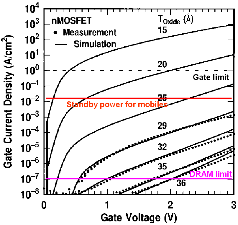
Figure 2915. Measured and simulated IG–VG characteristics (leakage current), with gate SiO2 layers in different thicknesses, under inversion conditions of nMOSFETs. The dotted line indicates the maximum tolerable gate leakage current would be of the order of 1 A/cm for a power supply of 1 V.
Adapted from [7]
However, in high k dielectric MOS structures in ICs, the metal gate oxides must not react with Si (silicon) to form either SiO2 or a silicide,
MO2 + Si = M + SiO2 ------------------------------- [2915a]
MO2 + 2Si = MSi + SiO2 ------------------------------- [2915b]
where,
M -- The metal element.
Chemical reaction Equation 2915a results in a SiO2 layer that has a lower dielectric constant than the high k material. Equation 2915b forms a silicide, resulting in electrical short failure.
[1] Wilk G, Wallace R M, Anthony J M, 2001 J. Appl. Phys. 89 5243
[2] Wallace R M and Wilk G D 2003 Crit. Rev. Solid State Mater. Sci. 28 231
[3] Robertson J 2004 Eur. Phys. J. Appl. Phys. 28 265
[4] Huff H and Gilmer D (ed) 2004 High K gate Dielectrics (Berlin: Springer)
[5] Houssa M (ed) 2003 High Dielectric Constant Materials: VLSI MOSFET Applications (London: IOP)
[6] Demkov A A and Navrotsky A (ed) 2005 Materials Fundamentals of Gate Oxides (Dordrecht: Springer)
[7] Lo S. H., Buchanan D. A., Taur Y. and Wang W., Quantum-Mechanical Modeling of Electron Tunneling Current from the Inversion Layer of Ultra-Thin-Oxide nMOSFET’s, (1997) IEEE Electron Device Lett. 18 209.
|