|
This book (Practical Electron Microscopy and Database) is a reference for TEM and SEM students, operators, engineers, technicians, managers, and researchers.
|
=================================================================================
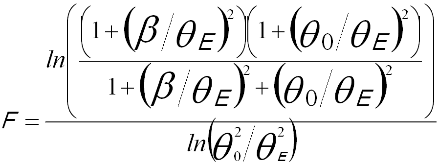
The fraction F of electron scattering (including both elastic and inelastic scatterings) at angles smaller than a scattering angle β can be given by, [1]
 --------------------------------- [2931] --------------------------------- [2931]
where,
θ0 -- (≈λZ1/3/(2πa0)) The soft cutoff to the Lorentzian angular distribution,
θE ≈ 0.5Em/E0 (non-relativistically)
Mkhoyan et al. [2] applied multislice method to simulate the angular distribution of scattered electrons at different thicknesses of amorphous Si specimens in STEM imaging. Under the optics conditions described in Figure 2575b, only ~60% of the original beam reachs the BF (bright-field) or EELS detector after passing through 100 nm (marked by the red line) of an a-Si specimen if a 21.5-mrad collection aperture is used, and only ~30% if an 8.5-mrad collection aperture is applied. Note that in EELS mode, the collection aperture normally refers to, for instance, the entrance aperture of GIF detector.
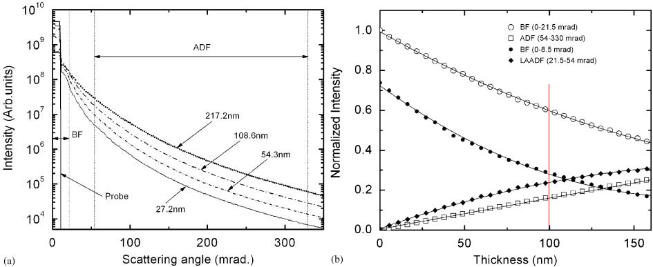
Figure 2575b. Simulated electron scattering in STEM after passing through a-Si specimens at different thicknesses: (a) Angular distribution of the scattered electrons; (b) Fraction of the scattered electrons of the incident beam into BF/EELS and ADF (annular dark field) detectors. The inner and outer angles of the ADF detector are indicated. Optics conditions are: STEM convergence angle = 10 mrad, Cs = 1.3 mm, and Δf = 85 nm.
Adapted from [2]
[1] F. Lenz, Z. Naturforsh 9A (1954) 185.
[2] K.A. Mkhoyan, T. Babinec, S.E. Maccagnano, E.J. Kirkland, and J. Silcox, Separation of bulk and surface-losses in low-loss EELS
measurements in STEM, Ultramicroscopy 107 (2007) 345–355.
|