EDS and WDS Measurements of Titanium - Practical Electron Microscopy and Database - - An Online Book - |
|||||||
| Microanalysis | EM Book http://www.globalsino.com/EM/ | |||||||
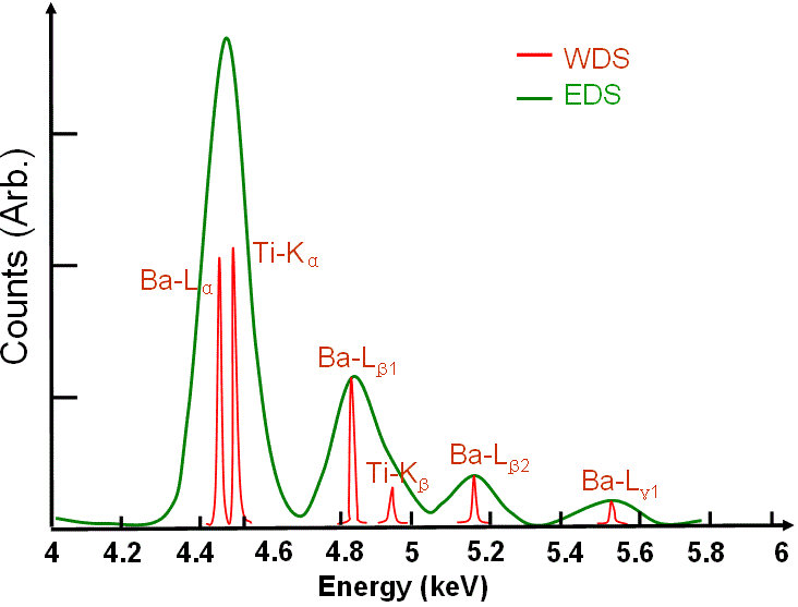
The EDS profile of BaTiO3 system shown in Figure 3108a presents an example of EDS peak overlap. For EDS measurements, the typical FWHM (full width at half maximum) intensity of the primary Ti lines (Kα 4.508 keV and Kβ 4.931 keV) is 160 eV at 30 kV of accelerating voltage. However, the FWHM of the WDS peaks is only a few eV because the energy resolution of the wavelength spectrometer is 5-10 eV. In this case, peak overlap in WDS is not a problem.
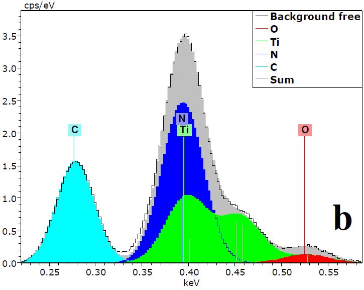
Figure 3108b shows the deconvolution of an EDX spectrum with peak overlaps, taken from a material that contains O, Ti, N, and C elements.
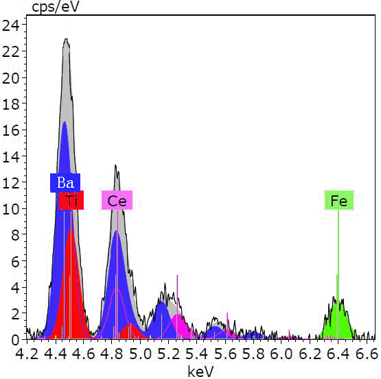
Figure 3108b. Deconvolution of an EDX spectrum with peak overlaps. [1] Figure 3108c shows a deconvoluted X-ray spectrum taken from a material containing Ba, Ti, Ce, and Fe elements. The different colored peaks represent the contribution of the various elements. The grey area is the background corrected spectrum which is the sum of all the deconvoluted lines.
With automatic elemental identification of NSS software, Ce cannot be identified. Instead, the software incorrectly suggests Ti, Fe, Co, Os, and Pb everywhere in elemental maps.
[1]
J. Berlin, T. Salge, M. Falke, and D. Goran, Recent Advances in EDS and EBSD Technology: Revolutionizing the Chemical Analysis of Chondritic Meteorites at the Micro- and Nanometer Scale, 42nd Lunar and Planetary Science Conference, 2723, (2011).
|
|
||||||