EM Simulation of Integrated Circuits - Practical Electron Microscopy and Database - - An Online Book - |
||||||||
| Microanalysis | EM Book https://www.globalsino.com/EM/ | ||||||||
| ================================================================================= | ||||||||
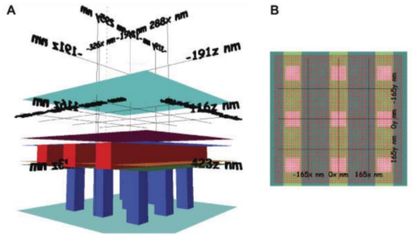
CASINO software has been used to simulate the interaction of the incident electron probe with the matter on a complex sample shown in Figure 1176. This simulated structure is a part of an integrated circuit, consisting of a typical CMOS stack layer for 32 nm technology node with different dielectric layers, copper (Cu) interconnects, and tungsten (W) via. The presence of the tungsten via will increase the BSE emission.

[1] Hendrix Demers, Nicolas Poirier-Demers, Alexandre Real Couture, Dany Joly, Marc Guilmain, Niels De Jonge And Dominique Drouin, Three-Dimensional Electron Microscopy Simulation with the CASINO Monte Carlo Software, CANNING 33, 135–146 (2011).
|
||||||||
| ================================================================================= | ||||||||
|
|
||||||||