EDS k-Factor Affected by Probe Size - Practical Electron Microscopy and Database - - An Online Book - |
||||||||
| Microanalysis | EM Book https://www.globalsino.com/EM/ | ||||||||
| ================================================================================= | ||||||||
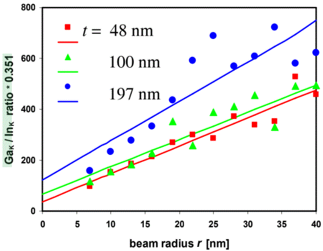
The k-factors in EDS measurements depend on many factors, e.g. the probe size of the incident electron beam. For instance, Figure 1181 shows the plot of the k-factor corrected Ga/In ratio of the K-lines, taken from a GaIn alloy, as a function of the probe radius (r) and TEM sample thickness (t).
Wood et al. [2] suggested that the x-ray absorption in the sample is not significant (<5%) when the probe size is larger than ~9 nm, while it shows significant absorption if the electron probe is smaller, e.g. in the range of 5-10 nm in diameter.
[1] T. Walther, A comparison of transmission electron microscopy methods to measure wetting layer thicknesses to sub-monolayer precision, Journal of Physics: Conference Series 126, 012091, (2008).
|
||||||||
| ================================================================================= | ||||||||
|
|
||||||||