EELS Artifacts Induced by High Beam Current - Practical Electron Microscopy and Database - - An Online Book - |
||||||||
| Microanalysis | EM Book https://www.globalsino.com/EM/ | ||||||||
| ================================================================================= | ||||||||
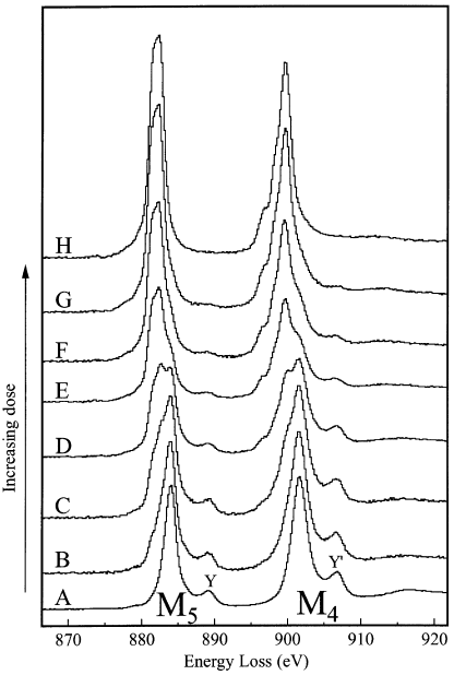
In some cases, EELS artifacts induced by beam damage on the specimens in TEM measurements can be monitored by observation of energy-loss near-edge structure (ELNES), for instance, in the damage process of CeO2 specimens. The electron beam damage induces the changes in the spectral shape of a CeO2 specimen in thickness of 0.17λ within a few seconds. λ is inelastic mean free path. Figure 1301 shows the damage sequence from fresh CeO2 (A) to damaged CeO2 (H) with such thickness. After H, the edge showed no further changes with increase of electron dose. The M5 and M4 maxima and the peaks Y and Y' are associated with Ce4+. The electron-beam damaged CeO2 presents Ce M4,5 and O K-edge shapes that are consistent with reduction to a Ce3+ oxide. During the beam-damage process the spectrum of CeO2 changes as below:
Figure 1301. The damage sequence from fresh CeO2 (A) to damaged CeO2 (H) in thickness of 0.17λ. The estimated doses in each case are (A) 3 x 10⁵ e/Å2; (B) 6 x 10⁵ e/Å2; (C) 2 x 10⁶ e/Å2; (D) 3 x 10⁶ e/Å2; (E) 7 x 10⁶ e/Å2; (F) 1 x 10⁷ e/Å2; (G) 2 x 10⁷ e/Å2; and (H) 5 x 10⁷ e/Å2. [1] [1] L.A.J. Garvie and P.R. Buseck, Determination of Ce4+/Ce3+ in electron-beam-damaged CeO2 by electron energy-loss spectroscopy, Journal of Physics and Chemistry of Solids 60 (1999) 1943–1947.
|
||||||||
| ================================================================================= | ||||||||
|
|
||||||||