| Figure 1309 shows the ion milling rate versus angle at a flux of 1 mA/cm2 750 eV argon (Ar) ions.
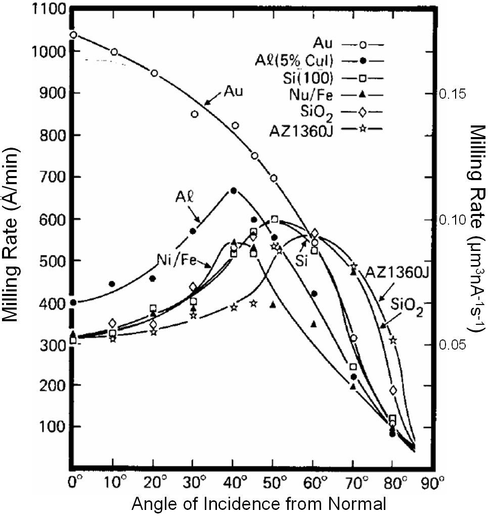
| Figure 1309. Ion milling rate versus angle at a flux of 1 mA/cm2 750 eV argon ions. Adapted from [5] |
Table 1309. Examples of milling rates of different materials with Ar ion polishing. The incident angle is the angle of incidence with respect to target normal.
| Sputtered material |
Milling rate
(µm3nA-1s-1 ) |
Total Yield (Atoms/Ion) |
| Beam energy: 2 kV and incident angle: 30° |
| Si |
0.0778 |
|
| Beam energy: 2 kV and incident angle: 15° |
| Si |
0.01667 [1] |
|
| Beam energy: 900 V and incident angle: 15° |
| Si |
0.0138 [1] |
|
| Beam energy: 500 V and incident angle: 15° |
| Si |
0.0041667 [1] |
|
| Beam energy: 500 V and incident angle: 0° |
| Ag |
0.366667 [3], 0.3 [4] |
|
| Al |
0.1216667 |
|
| Al2O3 |
0.01667 [3] |
|
| Au |
0.28333 [3], 0.18 [4] |
|
| Be |
0.028333 |
|
| C |
0.00733 |
|
| CaHNaO2 |
0.04875 |
|
| CdS |
0.38333 |
|
| Co |
0.091667 |
|
| Cr |
0.096667 [3], 0.08833 [4] |
|
| Cu |
0.183333 |
|
| Dy |
0.183333 |
|
| Er |
0.163333 |
|
| Fe |
0.088333 |
|
| GaAs (110) |
0.266667 |
|
| GaP (111) |
0.266667 |
|
| GaSb (111) |
0.316667 |
|
| Gd |
0.183333 |
|
| Ge |
0.166667 |
|
| Hf |
0.11 |
|
| InSb |
0.25 |
|
| Ir |
0.1 |
|
| LiNbO3 |
0.06667 |
|
| MgO |
0.02667 |
|
| Mo |
0.09 |
|
| Mo2C |
0.048333333 |
|
| Nb |
0.073333333 |
|
| Ni |
0.11 |
|
| Os |
0.085 |
|
| PbTe |
0.633333333 |
|
| Pd |
0.21667 |
|
| Pt |
0.14667 [3] |
|
| Re |
0.08667 |
|
| Rh |
0.12333 |
|
| Ru |
0.10167 |
|
| Si |
0.06333 [3] |
|
| SiC (0001) |
0.058333333 |
|
SiO2 |
0.0667, 0.065 [3], 0.0617 [4] |
|
| Sm |
0.183333333 |
|
| Sn |
0.3 |
|
| Ta |
0.07 |
|
| Th |
0.136666667 |
|
| Ti |
0.063333333 |
|
| U |
0.123333333 |
|
| V |
0.061666667 |
|
| W |
0.063333333 |
|
| Y |
0.16 |
|
YBa2Cu3O7 |
0.075 |
|
| ZnS |
0.1219 |
|
| Zr |
0.103333333 |
|
| Beam energy: 400 V and incident angle: 0° |
YBa2Cu3O7-x
|
0.008667
[2] |
|
| Beam energy: 200 V and incident angle: 0° |
| Ag |
0.166666667 |
|
| Al |
0.048333333 |
|
| Au |
0.118333333 |
|
| Be |
0.008666667 |
|
| C |
0.002166667 |
|
| CdS |
0.183333333 |
|
| Co |
0.043333333 |
|
| Cr |
0.055 |
|
| Cu |
0.088333333 |
|
| Dy |
0.096666667 |
|
| Fe |
0.043333333 |
|
| GaAs (110) |
0.13 |
|
| GaP (111) |
0.115 |
|
| GaSb (111) |
0.15 |
|
| Gd |
0.091666667 |
|
| Ge |
0.081666667 |
|
| Hf |
0.051666667 |
|
| InSb |
0.126666667 |
|
| Ir |
0.043333333 |
|
| Mo |
0.04 |
|
| Nb |
0.03 |
|
| Ni |
0.051666667 |
|
| Os |
0.033333333 |
|
| PbTe |
0.266666667 |
|
| Pd |
0.1 |
|
| Pt |
0.065 |
|
| Re |
0.038333333 |
|
| Rh |
0.051666667 |
|
| Ru |
0.04 |
|
| Si |
0.026666667 |
|
| Sm |
0.085 |
|
| Sn |
0.141666667 |
|
| Ta |
0.033333333 |
|
| Th |
0.068333333 |
|
| Ti |
0.026666667 |
|
| U |
0.056666667 |
|
| V |
0.028333333 |
|
| W |
0.03 |
|
| Y |
0.075 |
|
| Zr |
0.045 |
|
| |
|
|
| * The angles are the angles from normal incidence. |
[1] Arda Genç, Phase Stability in Metallic Multilayers, Ohio State University, Dissertation, 2008.
[2] Roman Adam, Stefan Benacka, Stefan Chromik, Marian Darula, Vladimir Strbik, and Stefan Gazi, Ivan Kostic, Emil Pincik, YBa2Cu3O7-x Step-Edge Junctions Prepared on Sapphire Substrates with YSZ Buffer Layer, IEEE Transactions on Applied Superconductivity, 5 (2), 1995.
[3] Williams, K., Gupta, K. & Wasilik, M. Etch rates for micromachining processingpart II. J. Microelectromech. S. 12, 761–778 (2003).
[4] Commonwealth Scientific Corporation. Ion beam etch rates. Bulletin 137-78.
[5] CHAPTER 3 Topography Effects in Deposition and Etching.
|
