Amorphous Layer Formed during EM Sample Preparation using Ar Milling - Practical Electron Microscopy and Database - - An Online Book - |
||||||||
| Microanalysis | EM Book http://www.globalsino.com/EM/ | ||||||||
| ================================================================================= | ||||||||
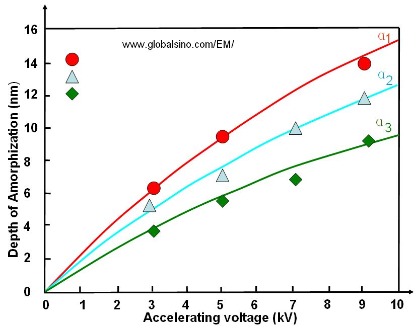
Figure 1428 shows that the thickness of the amorphization layer induced by Ar ion milling on sample surfaces can be reduced by lowering both the ion accelerating voltage and the incident ion-milling angle (α).
[1] McCaffrey J.P. et al Ultramicroscopy 87, 97, (2001).
|
||||||||
| ================================================================================= | ||||||||
|
|
||||||||