=================================================================================
Bridging (or called spiking) failure is very common in IC industry.
Ideally, Al (aluminum) would be deposited directly onto Si with perfect interfaces between Al and Si as shown in Figure 2016a (a). Unfortunately, the Si migrates into the Al, resulting in voids formed in the Si as shown in Figure 2016a (b). The Al can subsequently migrate into the formed voids, inducing spiking as shown in Figure 2016a (c). The big spike leads to junction shorts between n+ and p layers.
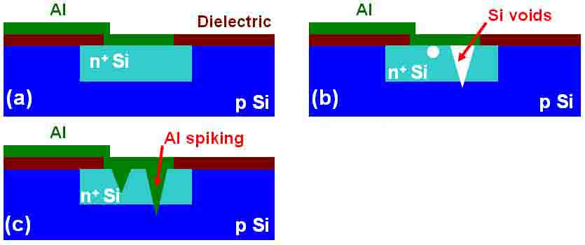
Figure 2016a. (a) Al deposited directly onto Si; (b) Voids formed in Si; and (c) Al spiking.
Figure 2016b shows several chemical reactions occurring during annealing of a transistor structure coated with Ti to form a low resistive TiSi2 layer at the source, gate, and drain. When silicon and titanium are reacted, Ti and Si can diffuse laterally over the isolation regions and form thin filaments of TiSix that can electronically connect a gate electrode and source/drain regions and can cause failure of the device. This phenomenon is called "bridging". On the other hand, those by-products (TiSix, TiOx, and TiN) form over the isolation regions and cannot easily be etched in conventional salicide etching solutions. The use of a nitrogen atmosphere during thermal annealing is essential in preventing this failure mechanism [1] because nitrogen quickly diffuses into the grain boundaries and significantly suppresses any long-range silicon diffusion in the titanium layer. Furthermore, to avoid the by-product formation, the annealing temperature cannot be too high.
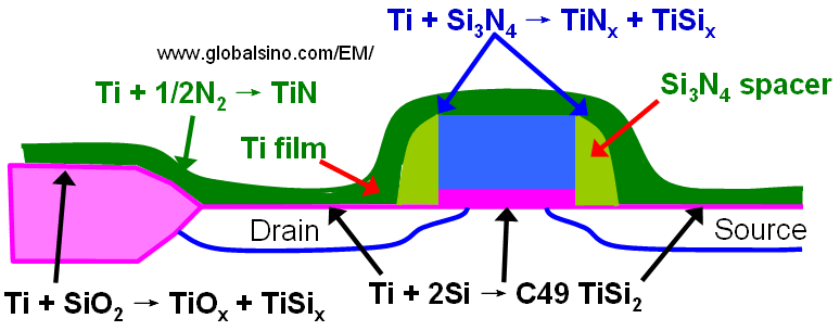
Figure 2016b. Several chemical reactions occurring during annealing of a transistor structure coated with Ti to form a low resistive SiTi2 layer.
[1] C. K. Lau, “Method of Forming Titanium Disilicide,”
U.S. Patent 4,545,116, 1985.
|