Chapter/Index: Introduction | A | B | C | D | E | F | G | H | I | J | K | L | M | N | O | P | Q | R | S | T | U | V | W | X | Y | Z | Appendix
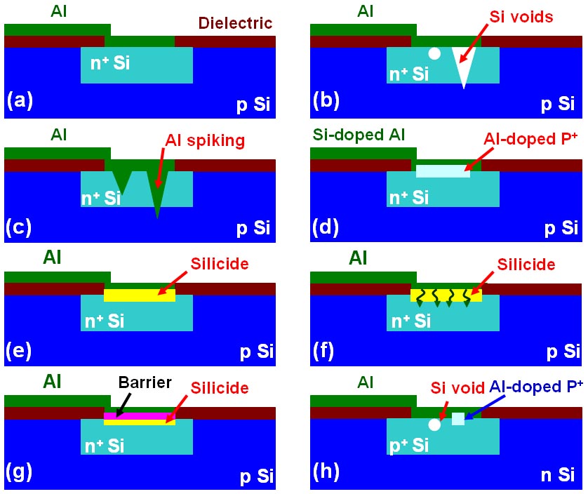
| In integrated circuits (ICs), conductive lines provide electrical interconnection among different parts of the ICs, devices, and the outside. The main applications of metallization are classified by gate, contact, and interconnection. Polysilicon and silicides are commonly applied as gates and interconnects in MOS devices. Figure 2036a shows the historical view of ohmic contact developments in Si(silicon)-based ICs. Ideally, Al (aluminum) would be deposited directly onto Si with perfect interfaces between Al and Si as shown in Figure 2036a (a). Unfortunately, the Si migrates into the Al, resulting in voids formed in the Si as shown in Figure 2036a (b). The Al can subsequently migrate into the formed voids, inducing spiking as shown in Figure 2036a (c). The big spike leads to junction shorts between n+ and p layers. Because the solubility of Si in Al is small (e.g. 0. 5 wt% at 450 °C), low Si doping in Al (1 to 3 wt% Si) suppresses spike formation significantly. However, other problems can occur subsequently, for instance, Al-doped p+ Si can precipitate out or p+ Si epitaxial layer can be formed between the original Si surface and the Al film as shown in Figure 2036a (d). Note that here Al is a p-type of dopants in Si. Furthermore, a challenge is that the formation probability of such epitaxial films is higher for (100)- than for (111)-oriented Si substrates. This can be more severe problem when the contact is scaled further and thus it only contains one or few grains. Note that titanium silicidation generates less silicon vacancies in the silicon substrate than by cobalt silicidation. [1] Silicides were introduced to solve the precipitation problem. As shown in Figure 2036a (e), a silicide is formed by depositing a metal onto Si, followed by heating the sample. Here, the Al does not have to be doped with Si. However, the Al above the silicide can still migrate through the silicide along the grain boundaries of the silicide, resulting in formation of Al/Si contacts as shown in Figure 2036a (f). This migration can be enhanced by the high compressive stress in the Al induced by its high CTE than that of Si (CTEAl>> CTESi) at high temperatures. Recently, barrier layers are introduced to address the migration problem as shown in Figure 2036a (g). These barrier layers have the properties of low contact resistance, and good chemical, electrical, and mechanical stabilities.
Figure 2036a. Historical view of ohmic contact developments in Si-based ICs: (a) Al deposited directly onto Si; (b) Voids formed in Si; (c) Al spiking; (d) p+ Si formation; (e) Silicides; (f) Formation of Al/Si contacts; and (g) Barrier layer/silicide.
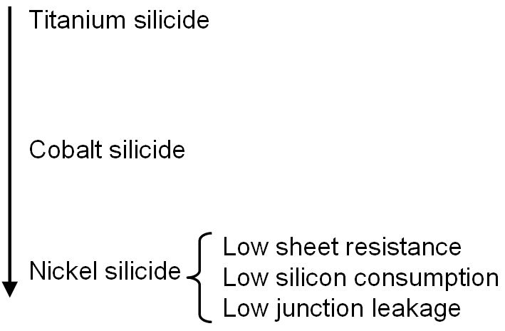
Figure 2036b shows the migration of silicide formation in semiconductor technology development.
Refractory metal silicides such as TiSi2, WSi2, TaSi2, and MoSi2 have been widely applied in Si technology because of their low resistivity and high temperature stability. TiSi2 among those silicides shows the lowest electrical resistivity (~12.4 µΩ cm). Table 2036a. Metallization selections in ICs.
In high k dielectric MOS structures in ICs, the metal gate oxides must not react with Si (silicon) to form either SiO2 or a silicide, MO2 + Si = M + SiO2 ------------------------------- [2036a] where, Chemical reaction Equation 2036a results in a SiO2 layer that has a lower dielectric constant than the high k material. Equation 2036b forms a silicide, resulting in electrical short failure. Some silicides can cause problems in IC devices. For instance, copper migrating into silicon active areas can form copper silicide precipitates resulting in leakage current at source and drain shallow junctions. Table 2036b. Desired properties of the suicides for integrated circuits. [3]
[1] S. B. Herner, K. S. Jones, H.-J. Gossmann, J. M. Poate, and H. S. Luftman,
Appl. Phys. Lett. 68, 1687 (1996).
|