=================================================================================
Electron diffraction patterns and Kikuchi patterns in both EBSD and CBED present similar geometry and can be successfully calculated using a Bloch-wave approach. The Bloch-wave is known from Bloch’s theorem for a translationally invariant scattering potential,
 ------------------- [2209a] ------------------- [2209a]
 ------------------- [2209b] ------------------- [2209b]
where,
cj and cg(j) -- Coefficients;
k(j) -- Vectors.
These coefficients and vectors can be obtained by solving Schrödinger equation by limiting the wave-function expansion to a number of Fourier coefficients labeled by the respective reciprocal lattice vectors g, coupling the incident electron beam to a diffracted beam. The eigenvalues λ(j) is obtained by re-writing the Bloch-wave vector k(j) as the sum of the incident beam wave vector K in the crystal and a surface normal component as k(j) = K + λ(j)n. Equation 2209b can be re-written by,
 ------------------- [2209c] ------------------- [2209c]
 ------------------- [2209d] ------------------- [2209d]
where,
t – The depth from the entrance surface of the sample.
The exponential term exp[2πi(K + g)·r] in Equation 2209d indicates the contributions of plane waves moving into the directions K + g. ϕg(t) gives the a depth dependent amplitude. The plane waves in directions K + g correspond to the diffracted beams that form a spot diffraction pattern.
Figure 2209a shows electron diffraction patterns of molybdenite (MoS2, molybdenum sulfide) taken at an incident electron beam energy of 500 kV from TEM samples in thicknesses of (a) 0.8 µm, (b) 2.0 µm, (c) 3.0 µm, and (d) 5.0 µm. For the thinnest TEM sample (0.8 µm), the diffracted spots are stronger than Kikuchi patterns, while the Kikuchi patterns are stronger than the spots for the case of 2.0 µm thick. Note that there are still two strong spots in the two beam condition (b). In the case with a thicker TEM sample in (c), the Kikuchi patterns are mainly shown even though the main diffracted spots can still be recognized, but the spots become more and more elongated along the corresponding Kikuchi bands as the TEM sample thickness increases. For the case with a very thick TEM sample (d), the Kikuchi band is almost uniform even when the incident spot is positioned on the sides of the band.
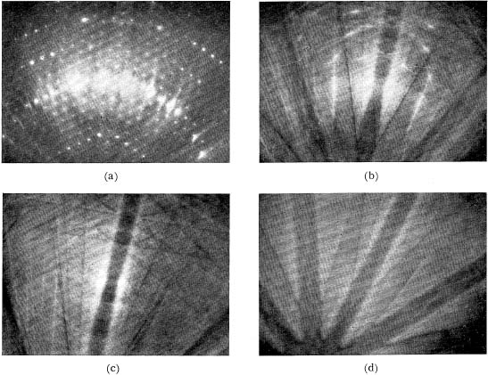
Figure 2209a. Electron diffraction patterns of molybdenite (MoS2, molybdenum Sulfide) taken at an incident electron beam energy of 500 kV from TEM samples in thicknesses of (a) 0.8 µm, (b) 2.0 µm, (c) 3.0 µm, and (d) 5.0 µm. [1]
Figure 2209b shows the dependence of the appearance of electron diffraction and Kikuchi patterns on the TEM sample thickness and the accelerating voltages of the incident electron beam for molybdenite crystals. Diffraction patterns can be observed in the region below Curve A, while Kikuchi patterns can be observed between Curves A and B. Both diffraction and Kikuchi patterns can be simultaneously observed in the region slightly below and above Curve A. In general, the Curve B gives the maximum thickness for which dislocations can be observable.
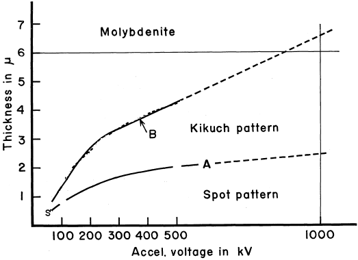
Figure 2209b. The dependence of the appearance of diffraction and Kikuchi patterns on the TEM sample thickness and the accelerating voltages of the incident electron beam for molybdenite crystals. Adapted from [1]
Figure 2209c shows the simulated, thickness-dependent CBED and EBSD patterns of Mo (001) crystals obtained with a 20 keV incident electron beam. Figure 2209c (a) shows CBED patterns simulated from Mo samples in thicknesses (t) of 1, 5, 10 and 50 nm. The pattern from the thinnest (1 nm) sample is very unsharp, while the patterns increase in sharpness up to 10 nm, with contributions from weaker reflections. Beyond this thickness, absorption effects take over so that it appears darker with increase of thickness. On the other hand, the intensity (I) of the patterns decreases from 0.7 to 0.002 with increase of the sample thickness. The EBSD patterns in Figure 2209c (b) look inverted by contrast and intensity with respect to the CBED patterns.
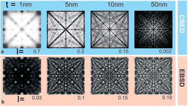
Figure 2209c. Simulated, thickness-dependent CBED and EBSD patterns of Mo
(001) crystals obtained with a 20 keV incident electron beam. Adapted from [1]
[1] Uyeda, Ryozi; Nonoyama, Minoru, The Observation of Thick Specimens by High Voltage Electron Microscopy. Experiment with Molybdenite Films at 50-500 kV, Japanese Journal of Applied Physics, 6(5), pp. 557 (1967).
|