Chapter/Index: Introduction | A | B | C | D | E | F | G | H | I | J | K | L | M | N | O | P | Q | R | S | T | U | V | W | X | Y | Z | Appendix
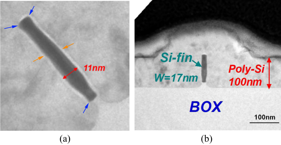
| Investigating individual point defects, such as monovacancies, using TEM-related techniques presents significant challenges due to the need for both atomic sensitivity and resolution. Additionally, specimens must be extremely thin to allow the detection of individual point defects through image contrast. The microscope's experimental conditions are also crucial for point defect analyses. For example, in a study analyzing monovacancies in single-layered h-BN (hexagonal boron nitride) using STEM-EELS with a JEM-2100F microscope (equipped with a delta corrector and a cold field emission gun) operated at 60 kV, a probe current of approximately 40 pA was applied. Achieving an EELS energy resolution of 200 meV or better is particularly difficult. Moreover, in many cases, it is challenging to eliminate the influence of thickness effects on the overall signal, such as at grain boundaries and rough interfaces. For the ultra-thin Si-fin structures shown in Figure 2225, several challenges exist in TEM analysis. One of the main concerns is the oxide quality, structure, and possible impurities in the oxide layer with a thickness of <3 nm, which are critical in determining the performance and reliability of devices like FinFETs. In many cases, In many cases, electrical shorts have been observed related to the structures such as FinFETs, where the short may occur within the oxide layer, or in areas or metal-lines electrically connected to the Si-fin or the Poly-Si gate. However, confirming the exact location of the short, particularly within the oxide, faces significant challenges. This difficulty arises due to the limitations of TEM and EELS in accurately determining the quality and uniformity of the oxide layer. TEM, while powerful for imaging, may not always reveal subtle electrical defects or impurities that could contribute to shorts, especially in amorphous oxide regions. Similarly, EELS is effective for compositional analysis but may struggle to detect fine variations in oxide quality that could lead to electrical failures. Measurement challenges in ultra-thin FinFET structures can arise, especially at the interfaces between the fin and gate, which are inherently complex due to their three-dimensional (3D) nature. Due to such 3D nature, the accuracy of measuring the oxide thickness can be challenging, and the actual oxide thickness can vary from 1 to 3 nm, or even 0 nm. Given that the fin dimensions are often less than 10 nm, the TEM samples need to be extremely thin for effective imaging, which introduces its own set of difficulties. During high-resolution TEM (HRTEM) imaging or EELS measurements, the nature of these ultra-thin samples makes them susceptible to damage. For instance, the electron beam used in HRTEM or EELS can induce structural changes, causing damage such as amorphization or local heating, which may alter the sample and affect the measurement accuracy. Furthermore, during TEM processing, voiding and evaporation may occur, leading to defects such as incomplete or damaged Si-fin structures. This is particularly problematic when attempting to study fine interface details or material properties, as the sample may degrade before critical data is collected. These challenges highlight the need for optimized sample preparation techniques and careful beam conditions during imaging to minimize the risk of damage while still obtaining high-quality data. Therefore, while these characterization techniques provide valuable structural and elemental information, they may not fully capture the electrical integrity of the oxide, making it difficult to definitively confirm if a short is located within the oxide layer or in another part of the device. This underscores the need for complementary electrical testing methods to identify the presence and exact location of shorts in such nanoscale devices. However, the techniques such as High-Resolution TEM (HRTEM), fine edge Electron Energy Loss Spectroscopy (EELS), and Extended Energy-Loss Fine Structure (EXELFS) are still essential for assessing the quality and distribution of oxide layers. Due to the potential damage from the electron beam during imaging, it is often necessary to use separate measurements for HRTEM and EELS in ultra-thin FinFET structures. That is, to mitigate this issue, one TEM sample may be dedicated to HRTEM measurements for analyzing grain orientation and structural properties within the Fin, while a second TEM sample with similar electrical properties is reserved for EELS measurements to assess compositional and chemical information. This approach ensures that the integrity of each sample is preserved for its respective analysis, reducing the risk of beam-induced damage that could compromise the results. By employing separate samples for HRTEM and EELS, researchers can obtain high-quality data for both structural and compositional analysis without sacrificing one for the other, ultimately leading to a more comprehensive understanding of the device characteristics. In addition, for such small-scale structures, STEM analysis can help in resolving the 3D arrangement and identifying crystalline and amorphous regions. TEM or failure analysts should also be aware that specific areas of a structure can present a higher probability of short-circuit failures. For instance, the corners marked by the blue arrows in the image can be more likely to cause shorts. This is because corners and edges often experience increased electric field stress, and their fabrication quality may be lower, making them more susceptible to breakdown or leakage pathways. These regions require careful inspection and may need design adjustments or additional protective measures to mitigate potential failures.
[1] Yue-Gie Liaw, Chii-Wen Chen, Wen-Shiang Liao, et al., Effects of ultra-thin Si-fin body widths upon SOI PMOS FinFETs, Modern Physics Letters B, 32(15):1850157, 2018.
|