=================================================================================
In practice, the strain analysis method using CBED technique has been applied to study the lattice strain distribution around local oxidation of silicon (LOCOS) in semiconductor devices at nanometer-scale spatial resolutions (e.g. 10 nm in diameter). For instance, Figure 2411 (a) shows a cross-sectional TEM image of a measured LOCOS region. The white circles are the points where the lattice strains are measured by CBED and are plotted against the distance from the field edge shown in Figure 2411 (b). The positive values represent tensile strain, while the negative values represent compressive strain. The tensile strain εxx (the normal strain in the x-direction) is attributed to the difference between the thermal expansion coefficients (CTE) of Si and SiO2. The Si CTE is ten times larger than that of SiO2. The smaller compressive strain εyy (the normal strain in the y-direction) indicates that the tensile stress in the x-direction acts on εyy compressively as lateral strain. The share strain εxy at the field edges is large probably due to dislocations formed near the LOCOS structure.
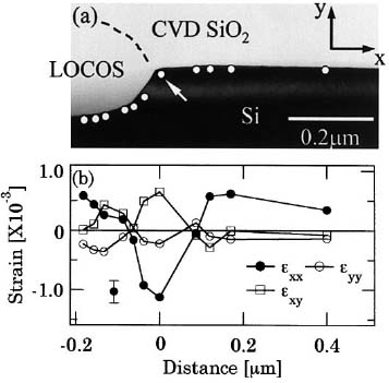
Figure 2411. (a) Cross-sectional TEM image of measured LOCOS region, and (b) The distribution of strain components as functions of the distance from the field edge. The position of the field edge is indicated by a white arrow.
[1]
Table 2411 lists main CMOS failure mechanisms in LOCOS (LOCal Oxidation of Silicon) technology.
Table 2411. Main CMOS failure mechanisms in LOCOS technology.
| LOCOS isolation |
Test polarity |
Pin pair (stress/reference) |
Failure mechanism |
Failure location |
[2] |
| N+ diffusion diodes |
Positive |
VSS |
Silicide penetration, metallurgical junction, contacts |
LOCOS bird's beak, metallurgical junction edge, contact-to-silicon surface |
[2] |
| P+ diffusion diodes |
Positive |
VDD |
Silicon melting, TiSi2 silicide resistance, contacts |
N-well under LOCOS, silicide surface |
[2] |
| N-well diodes |
Negative |
VSS |
Metallurgical junction failure |
|
[2] |
| N-well to n-well |
Negative |
Well-to-well |
Molten silicon |
LOCOS isolation between wells |
[2] |
| N-channel MOSFET |
Positive |
Drain-to-source |
MOSFET second breakdown |
Molten silicon, MOSFET channel region |
[2] |
| Positive |
Gate |
Gate dielectric failure |
MOSFET gate |
[2] |
| P-channel MOSFET |
Negative |
Drain-to-source |
MOSFET second breakdown |
Molten silicon, MOSFET channel region |
[2] |
| Negative |
MOSFET gate |
Gate dielectric failure |
MOSFET gate |
[2] |
N-well resistors
|
|
|
Resistor second breakdown |
Resistor metallurgical junction, contacts |
[2] |
| N-well ballasted n-channel MOSFET |
Positive |
Drain-to-source |
MOSFET second breakdown |
Molten silicon |
[2] |
| Positive |
Gate |
Gate dielectric failure |
MOSFET gate |
[2] |
[1] Akio Toda, Nobuyuki Ikarashi, Haruhiko Ono, Local lattice strain measurements in semiconductor devices by using convergent-beam electron diffraction, Journal of Crystal Growth 210 (2000) 341-345.
[2] Steven H. Voldman, ESD: Failure Mechanisms and Models, 2009.
|