|
This book (Practical Electron Microscopy and Database) is a reference for TEM and SEM students, operators, engineers, technicians, managers, and researchers.
|
=================================================================================
Ultra-thin (less than 20 nm), uniform, and damage-free TEM specimen without curtaining can be prepared using backside FIB milling method. Figure 2723a (a) shows a modified FIB stub with a 2nd probe on it for backside milling. The application of the modified FIB stub has advantages over the conventional methods because it allows efficient, fast, and precise sample flipping over 180 degrees. The operation procedure is:
i) The sample is first lifted out of the bulk sample by the 1st probe as shown in Figure 2723a (b),
ii) The sample is attached in situ to the 2nd probe, which is pre-fixed on the stub, as shown in Figure 2723a (c) and (d),
iii) The sample holder is unloaded and the modified stub is flipped over (180 degrees as shown in Figure 2723a (e)) so that the sample on the 2nd probe is also flipped upside down and thus the backside FIB milling can be done later,
iv) The sample is detached from the 2nd probe with the 1st probe as shown in Figures 2723a (f) and (g),
v) The sample is attached on the Cu grid using the 1st probe as shown in Figure 2723a (h).
vi) The sample is milled from the bottom of the wafer.
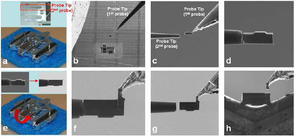
Figure 2723a. Sample stub and operation procedure of the backside milling: (a) Modified stub, (b) Sample extraction from the die, (c) The 2nd probe attached, (d) the 1st probe detached, (e) Invert stub 180 °, (f) The 1st probe attached, (g) The 2nd probe detached, and (h) Attach on Cu grid using the 1st probe. [1]
In the final milling, low kV was sequentially employed at 5 kV, 2 kV, and 1 kV on both sides of the sample. In the final cleaning, a FIB beam of 1 kV and 14 pA with an incident angle of 5 degree is used. Figure 2723b shows TEM images of NAND flash samples prepared by the conventional method (a) and the backside FIB milling method (b). In Figure 2723b (a), the sample thickness was 30 nm, while in Figure 2723b (b) the sample thickness was 20 nm so that there were no overlapping artifacts in the area of shallow trench isolation (STI).
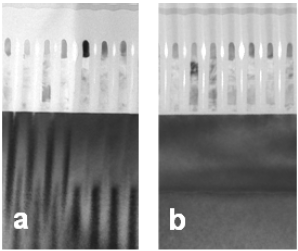
Figure 2723b. TEM images of NAND flash samples prepared by
the conventional method (a) and the backside milling
method (b). [1]
[1] Hyo-jin Kang, Jong Hyeop Kim, Jang won Oh, Tae Sun Back, and Ho Joung Kim, Ultra-Thin TEM Sample Preparation with Advanced Backside FIB Milling Method, Microsc. Microanal. 16 (Suppl 2), (2010) 170.
|