|
|
Deep Level States in Band Gap Analyzed by EELS
- Practical Electron Microscopy and Database -
- An Online Book -
|
|
https://www.globalsino.com/EM/
|
|
This book (Practical Electron Microscopy and Database) is a reference for TEM and SEM students, operators, engineers, technicians, managers, and researchers.
|
=================================================================================
In many cases, the deep level states in semiconductors can be analyzed by EELS measurements. For instance, the pronounced shoulder below 100 eV indicated by the arrow in Figure 2804 presents a deep level state, above Fermi level in band gap, produced by symmetric segment a 5-fold coordinated atom in CSL junction in polycrystalline silicon. The shoulder in the Si-L2,3 ELNES was detected only from the symmetric segment of the {112} Σ3 CSL boundary near the CSL junction, but not from the bulk, {112} and {111} Σ3 CSL boundaries. The CSL junction would be electrically active and affects the electrical conductivity in polycrystalline silicon.
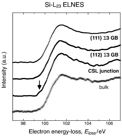
Figure 2804. The energy-loss near-edge spectra (ELNES) of Si-L2,3 edge acquired from a bulk, {112} and {111} Σ3 CSL boundaries, and their junction.
[1]
[1] Norihito Sakaguchi, Makito Miyake, Seiichi Watanabe, and Heishichiro Takahashi, EELS and Ab-Initio Study of Faceted CSL Boundary in Silicon, Materials Transactions, 52(3) (2011) 276.
|
=================================================================================
The book author (Yougui Liao) welcomes your comments, suggestions, and corrections, please click here for submission. If you let book author know once you have cited this book, the brief information of your publication will appear on the “Times Cited” page.
|
|