|
|
Nanoprobing Technique for IC Failure Analysis
- Practical Electron Microscopy and Database -
- An Online Book -
|
|
https://www.globalsino.com/EM/
|
|
This book (Practical Electron Microscopy and Database) is a reference for TEM and SEM students, operators, engineers, technicians, managers, and researchers.
|
=================================================================================
SEM (scanning electron microscopy)-based nanoprobing technique [1] is frequently used to identify the soft failure and non visible defects. This technique provides the capability of operating probe tips in nanometer range to land exactly on top of the individual source, drain and gate tungsten contact, for instance, as shown in Figure 2825. The SEM provides a high-resolution real-time image that facilitates locating the failing device and placing the probe tips. In this way, the locations of soft failure and non visible defects can become visible during electrical stressing.
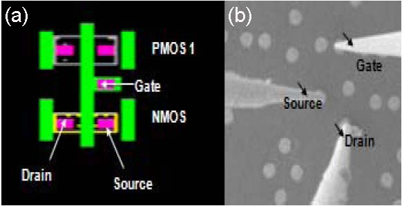
Figure 2825. (a) Inverter image, and (b) A SEM image showing three tungsten probes (black arrow) landing on tungsten contacts of the NMOS transistor in the inverter.
Adapted from [2]
[1] D. Faure, C.A. Waggoner, “A New Sub-micron Probing
Technique for Failure Analysis in Integrated Circuits”,
ESREF 2002.
[2] Ravikumar V K, Ho M Y, Goruganthu R R, Phoa S L, Narang V, Chin J M, Combining High Resolution Pulsed TIVA and Nanoprobing Techniques to identify Drive Strength issues in Mixed Signal Circuits, 2010 17th IEEE International Symposium on the Physical and Failure Analysis of Integrated Circuits (IPFA).
|
=================================================================================
The book author (Yougui Liao) welcomes your comments, suggestions, and corrections, please click here for submission. If you let book author know once you have cited this book, the brief information of your publication will appear on the “Times Cited” page.
|
|