=================================================================================
Thermally Induced Voltage Alteration (TIVA) is one type of Thermal Laser Stimulation (TLS) techniques. TIVA technique is widely recognized as a fast and effective tool for defect isolation in semiconductor devices. In this technique, a laser beam with wavelength below the semiconductor bandgap serves as an active probe to scan and to locally heat an integrated circuits (ICs) and then, the temperature rise (ΔT) in the ICs creates local changes in resistance. A constant current source supplies bias (Ibias) that results in thermal gradient and then voltage variation with the resistance changes. In the TIVA method, the voltage variation can be given by,
ΔVbias = TCR*ΔT*R0*Ibias ---------------------------- [2836a]
where,
TCR -- The local thermal coefficient of resistance,
ΔT -- The temperature change resulting from IR laser
beam scanning,
R0 -- The resistance of the IC,
Ibias -- The constant supply current.
Such resistance changes are captured when monitoring the voltage changes (ΔVbias) across the constant current (Ibias) supply pins. A digital record of changing voltage of the constant current source superimposes the image of the position of the focused and scanned laser beam, producing a TIVA image of the short-circuit defects. Therefore, the open/short defect in the current-biased device can be located.
TIVA laser can be equipped with two wavelengths: 1.34 µm for Silicon ICs and 1.064 µm for III-V material. The main TIVA applications are localizations of shorted signal lines, high resistive defects in conductors (e.g. voids), junction failure, and metallization defects. A limitation is that TIVA signal might be blocked by other metallic layers.
For silicon IC measurements, the lasers with 1340 nm wavelength (0.925 eV) eliminate the LIVA (light-induced voltage alteration) signal because it cannot induce electron and hole pairs, as a consequence of which the energy of the photons is below that of the Si (silicon) indirect band-gap (~1.12 keV for Si, see EM/page4635). The photocurrent effects from e-h (electron-hole) pair generation by the 1064 nm laser used in LIVA produce signals 1 to 2 orders of magnitude larger than the SEI and TIVA signals so that the 1064 nm laser should be avoided in SEI and TIVA measurements. Note that some lasers with 1340 nm wavelength still contain a weak intensity (e.g. < 1%) of light with 1047 nm wavelength; therefore, a long wavelength pass filter needs to be placed in the beam path in order to eliminate the unwanted LIVA signals.
In TIVA operation, the
sample was biased with constant current, and the voltage was
monitored. As the laser hit the defect location, then the resistance
will change due to thermal effect. Then the measured voltage
will change accordingly. In this case, the location was recorded and
correlated to the sample.
Figure 2836 shows the TIVA setup. The amplifier is operated in AC-coupled mode so that only the variations in VDD are recorded to show defective locations.
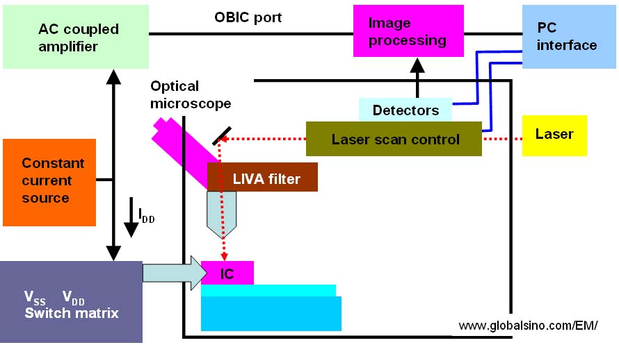
Figure 2836. TIVA setup. OBIC stands for optical beam induced current.
|