Chapter/Index: Introduction | A | B | C | D | E | F | G | H | I | J | K | L | M | N | O | P | Q | R | S | T | U | V | W | X | Y | Z | Appendix
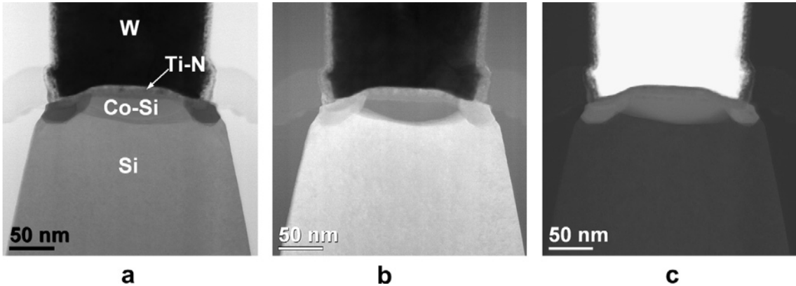
| Figure 4635 shows bright field (BF), annular dark field (ADF) and high angle annular dark field (HAADF) STEM images of a W/TiN/Co-Si/Si stack. In this analysis, Scanning Transmission Electron Microscopy (STEM) imaging techniques were employed to reveal key structural and compositional details. The BF STEM image highlights variations in transmitted electron intensity, providing insight into material structure and thickness variations within the stack. The ADF STEM image, which captures scattered electrons, improves the contrast and facilitates easier identification of distinct layers within the stack. In addition, the HAADF STEM image, known for its Z-contrast, enhances the visibility of heavier elements by capturing electrons scattered at high angles, where elements with higher atomic numbers appear brighter. This method is especially valuable for identifying compositional differences, allowing precise mapping of material distributions in the stack, which is critical for understanding performance and potential failure mechanisms in semiconductor devices. These complementary imaging modes provide a detailed view of the W/TiN/Co-Si/Si stack, aiding in process development and failure analysis.
[1] Raghaw S. Rai and Swaminathan Subramanian, Role of transmission electron microscopy in the semiconductor industry for process development and failure analysis, Progress in Crystal Growth and Characterization of Materials, 55, pp.63-97, 2009.
|