=================================================================================
Figure 2920 shows the scaling of feature size, gate length and oxide thickness of complementary metal oxide semiconductor (CMOS) field effect transistor (FET) made
from silicon according to the 2003 International Technology Roadmap for Semiconductors.
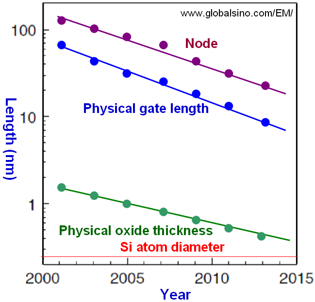
Figure 2920. Scaling of feature size, gate length and oxide thickness of CMOS-FET according to the 2003 International Technology Roadmap for Semiconductors.
The people now believe that the scaling limit to Moore’s law is lithography because of the need for shorter wavelengths of light to pattern the smaller feature sizes. Therefore, materials are now a key constraint in silicon technology. For example, the current density of conductors in ICs can be increased by using copper instead of aluminium. The RC time delays can be minimized using materials with lower dielectric constants instead of SiO2. Leakage in MOS structures can be minimized using materials, with high dielectric constants, between the gate and the silicon channel in FET in stead of SiO2.
|