|
This book (Practical Electron Microscopy and Database) is a reference for TEM and SEM students, operators, engineers, technicians, managers, and researchers.
|
=================================================================================
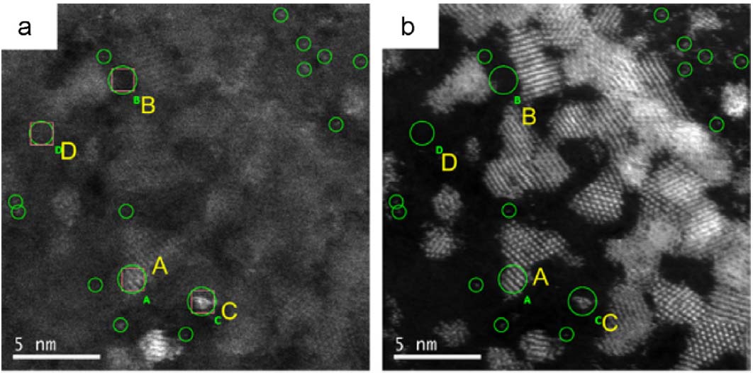
High resolution SEM observations were performed on a limited number of crystals such as Pd, Pt, Au, Ba, Y, Sr, Cu, Ti, Si, Mg, C, uraniu moxide (UO2), and SrTiO3 [4]. In those analyses, their lattice fringes were observed, in specimen thicknesses from a couple of nm to 20 nm, in SEM mode in Cs corrected Hitachi HD 2700C. Figure 2938 shows an example of SEM/STEM images taken from uranium oxide particles on carbon film at atomic resolution in both SEM mode and ADF-STEM mode. It is clear that the contrast of STEM is much better than that of SEM.

Figure 2938. SEM/STEM images taken from uranium oxide particles on carbon film at atomic resolution in SEM mode (a) and ADF-STEM mode(b).
[4]
To obtain high resolution SEM images, we need to have thin films similar to TEM observations. However, in many cases, this type of imaging cannot be successful because of charging of the thin specimens. Howie [1] and Liu and Cowley [2,3] summarized how to achieve nm-range resolution in thin specimens.
[1] A. Howie, J. Microsc. 180 (1995) 192.
[2] J. Liu, J.M. Cowley, Scanning Microsc. 2 (1988) 65.
[3] J. Liu, J.M. Cowley, Scanning Microsc. 2 (1988) 1957.
[4] H. Inada, D.Su, R. F. Egerton, M.Konno, L.Wu, J.Ciston, J.Wall, Y.Zhu, Atomic imaging using secondary electrons in a scanning transmission electron microscope: Experimental observations and possible mechanisms, Ultramicroscopy 111(2011)865–876.
|
