Failure Analysis of IC Devices - Practical Electron Microscopy and Database - - An Online Book - |
||||||||
| Microanalysis | EM Book http://www.globalsino.com/EM/ | ||||||||
| ================================================================================= | ||||||||
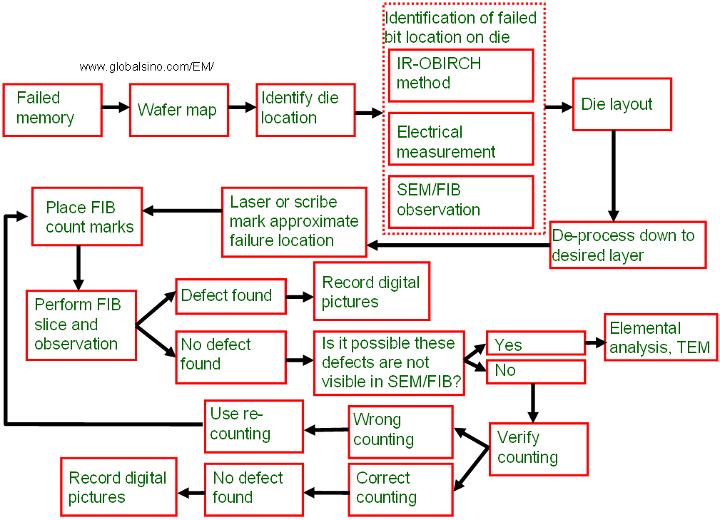
Failure analysis of IC (integrated circuit) chips is critical not only for trouble-shooting and problem-solving, but also for assurance of on-time delivery of products to market. In general, failure analysis includes electrical failure analysis (EFA) and physical failure analysis (PFA). The defects in IC devices and the related failure analysis can be very complicated and be categorized as listed in a table on page3291. The key to successful failure analysis depends highly on the effective fault isolation technique to root cause of failure and providing the physical manifestation of defect. [1] Some types of defects can be identified by in-line metrology, while more cannot due to scaling. Therefore, failure analysis after full fabrication process becomes more important. In many cases, the passivation and metal overlayers have to be polished off for localization and identification of the failure sites. This polishing process is so-called de-processing. Furthermore, this analysis can be very time-consuming because, especially in most cases, the analyst does not have adequate defect-coordinate. In such failure analysis, the analyst needs a wafer map and the layout of the chip, as well as the results of electrical measurements. As an example, Figure 3296 shows schematic illustration of failure analysis of memories.
Figure 3296. Schematic illustration of failure analysis of memories. In summary, the microelectronic failure analysis process is composed of
five main steps:
[1] Schlangen, R., Deslandes, H., Lundquist, T., Schmidt, C., Altmann, F., Yu, K., Andreasyan, A., & Li, S. (2010). Dynamic lock-in thermography for operation modedependent thermally active fault localization. Microelectronics Reliability, 50, 1454-1458.
|
||||||||
| ================================================================================= | ||||||||
|
|
||||||||