=================================================================================
In EELS analysis of boron (B) element, K-edge (188 eV), which is normally used, is in the low energy range in a spectrum, and thus background extraction is often challenging. For instance, for NixBy alloy, the large Ni M-edges (see page4771) causes problems in background fitting, for boron analysis, with the power-law fit, resulting in very low peak-to-background (P/B) ratios. In this case, only poor detection sensitivity (5–10 at.%) can be obtained for boron EELS analysis. [8]
Figure 3377a shows the B-K EELS edges of B (boron), B2O3 and Ni2B. The measured near edge structure for B2O3 is characterized by a sharp peak at 194 eV associated with transitions to non-bonding π* (Pz) orbitals, and a broad feature at ~ 203 eV originated from σ* orbitals.
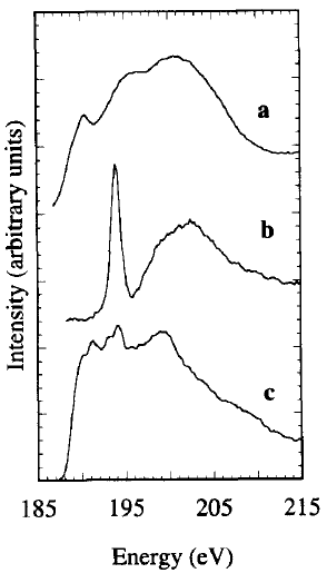
Figure 3377a. B-K EELS edges of B (boron) (a), B2O3 (b), and Ni2B (c). [1]
The B (boron) K edges of the Be-B-bearing materials present a wide range of shapes, reflecting their different bonding types. Those bonding types affect the electrical resistivity of the materials. These properties include metallic in Be2B (12 x 10-6 Ω cm), BeB2C2 (17 x 10-4 Ω cm), and BeB2 (2 x 10⁻² Ω cm); semiconducting in Be0.5B6C (3.3 Ω cm); and insulating in BeB6 and BeB8 to 12 (1 to 6 x 10⁷ Ω cm) [4]. Figure 3377b shows the B K edges of some B-bearing materials.
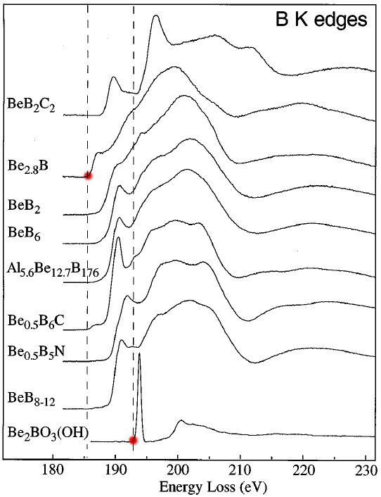
Figure 3377b shows the B K edges of some B-bearing materials. The dotted vertical lines label the lowest energy onset in metallic Be2.8B (≈Be3B) and the greatest energy onset in insulating Be2BO3(OH), also see the red dots. The dotted lines have been set to the inflection points of the rising edges.
Adapted from [5]
The EEL spectra in Figure 3377c presents boron(B)-bonding to other elements in Co–Rux–B-O catalysts. For the xRu = 0 sample, the spectrum shows both contributions of B-Co bonds and B-O bonds. For 0.13≤ xRu ≤ 0.7, the B-K edge is dominated by the signals from B-O bonds together with a smaller contribution of B-M (metals) bonds. For the xRu = 1 sample, the B-K edge shows the B–Ru bonds and a wide peak attributed to B-O bonds.
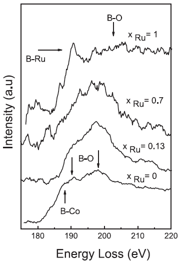
Figure 3377c. B K edges in the EELS spectra of Co–Ru–B-O catalysts.
[6]
Figure 3377d (a) shows a HAADF-STEM image of single-layered h-BN (hexagonal boron-nitride) and Figure 3377d (b) is a corresponding atomic model where a EELS linescan has been recorded, shown in (c) and (d). The STEM contrast of the N and B locations is determined by the atomic number, called Z-contrast. Figure 3377d (c) and (d) shows the EELS profiles of the boron K-edge and nitrogen K-edge signals, respectively. The N K-edge intensity does not go down to zero even between two nitrogen atoms because of EELS signal delocalization [2]. The large probe tail and mechanical instabilities such as the specimen drift during the line scan may also partially contribute to the nonzero intensity but this should not be a dominant effect because the simultaneously recorded STEM profile clearly shows well-separated atoms similar to the STEM signal presented in Figure 3377d (a).
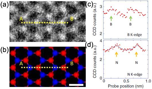
Figure 3377d. (a) A HAADF-STEM image of single-layered h-BN (hexagonal boron-nitride), (b) A corresponding atomic model where an EELS linescan was recorded (red: nitrogen, blue: boron), and (c) and (d) the EELS profiles of the boron K-edge and nitrogen K-edge signals. Adapted from [3]
In Figure 3377d (c) and (d), the boron EELS maxima are less visible in comparison with the nitrogen profile so that it is more difficult to see the atomic maxima in the boron K-edge profile rather than in the nitrogen case. This difference can be interpreted by the energy-loss dependence of EELS signal delocalization and the delocalizations for the boron K edge and for the nitrogen K-edge are 0.15 and 0.08 nm, respectively.
EEL spectrum shown in Figure 3377e was obtained from BN nanotubes prepared by continuous laser ablation of BN targets. It presents
five different edges, including B, C, Ca, N and O.
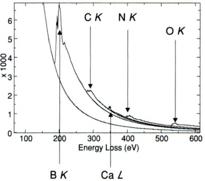
| Figure 3377e. EEL spectrum obtained from BN nanotubes prepared by continuous laser ablation of BN targets. [7] |
[1] G. Mountjoy, A. Corrias, P.H. Gaskell, An electron energy loss spectroscopy study of Ni60B40 alloys prepared by chemical reduction and melt spinning, Journal of Non-Crystalline Solids 192 & 193 (1995) 616-619.
[2] D. A. Muller and J. Silcox, Ultramicroscopy 59, 195 (1995).
[3] Kazu Suenaga, Haruka Kobayashi, and Masanori Koshino, Core-Level Spectroscopy of Point Defects in Single Layer h-BN, Physical Review Letters, 108, 075501 (2012).
[4]
V. S. Neshpor and G. V. Samsonov, Inorg. Mater. 7, 45 (1971).
[5] Laurence A. J. Garvie, Peter R. Buseck, and Peter Rez, Characterization of Beryllium–Boron-Bearing Materials by Parallel Electron Energy-Loss Spectroscopy (PEELS), Journal of Solid State Chemistry 133, 347-355 (1997).
[6] G.M. Arzac, T.C. Rojas, A. Fernández, New insights into the synergistic effect in bimetallic-boron catalysts for hydrogen generation: The Co–Ru–B system as a case study, Applied Catalysis B: Environmental 128 (2012) 39– 47.
[7] Nan Yao, Zhong Lin Wang, Handbook of Microscopy for Nanotechnology, 2005.
[8] C. C. Ahn, Transmission Electron Energy Loss Spectrometry in Materials Science and the EELS ATLAS, (2004).
|