=================================================================================
Figures 3379a show the features of dislocations in SiGe epitaxial films on Si substrates depending on the sizes of the active areas of microelectronic devices. The black surroundings are Si substrate. The arrows indicate the dislocation loops at the edge of the active area.
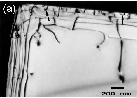 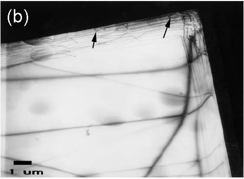
Figure 3379a. Dislocations in large active areas (37 µm x 180 µm): (a) Stressed-isolation wafer; (b) Stressed isolation wafer with 0% Ge after the 950 °C anneal. Note the density of dislocations at the isolation edge is high and there is no dislocations in the center region. Adapted from [1]
Figure 3379b shows a TEM (-220) bright field image taken from a photo-degraded CdxZnl-xSe/ZnSxSel-x heterostructure. This figure presents extended networks of dislocation tangles along the <100> directions corresponding to the two DLDs. The DLDs consist of extended dislocation loops. A small faulted defect labeled b was blocked by a large stacking fault labeled T during photodegradation. Along the trace of the faulted defect, very small dislocation loops (marked by arrowheads) were formed.
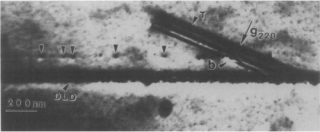
Figure 3379b. A TEM (-220) bright field image taken from a photo-degraded CdxZnl-xSe/ZnSxSel-x heterostructure. [2]
[1] K. Schonenberg, Siu-Wai Chan, D. Harame, M. Gilbert, C. Stanis and L. Gignac, The stability of Si1−xGex strained layers on small-area trench-isolated silicon, Journal of Materials Research, 12(02) (1997), pp 364-370.
[2] L. Salamanca-Riba and L.H. Kuo, Observation of [100] and [010] Dark Line Defects in Optically Degraded ZnSSe-Based LEDs by Transmission Electron Microscopy, Journal of Electronic Materials, 25 (2) (1996) 239.
|