=================================================================================
Figure 3393a shows nitrogen (N) map of MOSFET structure taken by an energy filter in EFTEM. The bright areas show N element, while the gray and dark areas were from other materials, such as SiO2, silicon (Si) substrate, and polycrystalline Si.
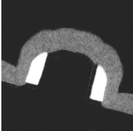
Figure 3393a. N map of MOSFET structure taken by an energy filter. [1]
Figure 3393b (a) shows a HAADF-STEM image of single-layered h-BN (hexagonal boron-nitride) and Figure 3393b (b) is a corresponding atomic model where a EELS linescan has been recorded, shown in (c) and (d). The STEM contrast of the N and B locations is determined by the atomic number, called Z-contrast. Figure 3393b (c) and (d) shows the EELS profiles of the boron K-edge and nitrogen K-edge signals, respectively. The N K-edge intensity does not go down to zero even between two nitrogen atoms because of EELS signal delocalization [2]. The large probe tail and mechanical instabilities such as the specimen drift during the line scan may also partially contribute to the nonzero intensity but this should not be a dominant effect because the simultaneously recorded STEM profile clearly shows well-separated atoms similar to the STEM signal presented in Figure 3393b (a).
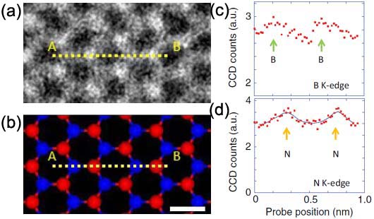
| Figure 3393b. (a) A HAADF-STEM image of single-layered h-BN (hexagonal boron-nitride), (b) A corresponding atomic model where an EELS linescan was recorded (red: nitrogen, blue: boron), and (c) and (d) the EELS profiles of the boron K-edge and nitrogen K-edge signals. Adapted from [3]. |
In Figure 3393b (c) and (d), the boron EELS maxima are less visible in comparison with the nitrogen profile so that it is more difficult to see the atomic maxima in the boron K-edge profile rather than in the nitrogen case. This difference can be interpreted by the energy-loss dependence of EELS signal delocalization and the delocalizations for the boron K edge and for the nitrogen K-edge are 0.15 and 0.08 nm, respectively.
Figure 3393c shows the comparison of the extracted EELS spectra of the N K-edge at 401 eV from a same region with the electron beam current of 150 pA and 850 pA, respectively, and from a crystalline TiN standard sample. Table 3393 shows the comparison of π* pre-peaks of the three cases in Figure 3393c. This split is caused by the excitation of an N 1s electron in unoccupied t2g and eg orbitals formed by the hybridization of N 2p and Ti 3d electrons. [4] The high electron beam flux of 850 pA used for the data acquisition changed the chemistry and morphology in the analyzed region.
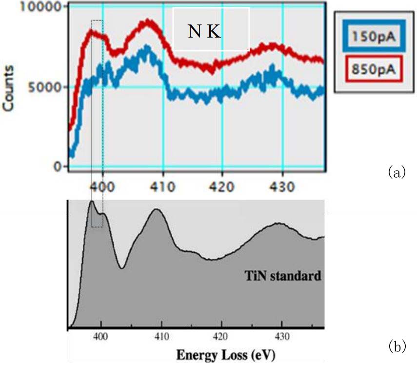
| Figure 3393c. Extracted EELS spectra of TiN: (a) With an electron beam current of 150 pA, (b) With an electron beam current of 850 pA and (c) from a crystalline TiN standard sample. [4] |
Table 3393. π* pre-peak of the three cases in Figure 3393c.
| |
π* pre-peak |
| With an electron beam current of 150 pA |
Appears to be weaker and no split |
| With an electron beam current of 850 pA |
Appears to be much stronger and more defined and is split by 2 eV |
| From a crystalline TiN standard sample |
[1] M. Worch, H.J. Engelmann, W. Blum, E. Zschech, Cross-sectional thin film characterization of Si compounds in semiconductor device structures using both elemental and ELNES mapping by EFTEM, Thin Solid Films 405 (2002) 198–204.
[2] D. A. Muller and J. Silcox, Ultramicroscopy 59, 195 (1995).
[3] Kazu Suenaga, Haruka Kobayashi, and Masanori Koshino, Core-Level Spectroscopy of Point Defects in Single Layer h-BN, Physical Review Letters, 108, 075501 (2012).
[4] P. Longo, H. Zhang and R.D. Twesten, Simultaneous DualEELS and EDS Analysis Across the Ohmic Contact Region in FinFET Electronic Devices – Exploring the Effects of Electron Beam Damage, Microsc. Microanal. 22 (Suppl 3), 2016.
|