|
This book (Practical Electron Microscopy and Database) is a reference for TEM and SEM students, operators, engineers, technicians, managers, and researchers.
|
=================================================================================
Some elemental losses due to radiation damage induced by the incident electron beam in EMs can be detected by EDS ratio technique. For instance, the elemental variation of k-factor kNaSi as a function of electron irradiation time for a thin specimen of Amelia albite (NaA1Si3O8) [1] indicated an elemental loss. The EDS data were obtained with an AEI EM6G system, operating at 100 kV, beam current 200 µA, and probe diameter 3 µm. Note that this current density is far below those available on modern analytical electron microscopes so that we need to pay attention to the potential damage when we are working on EDS measurements. On the other hand, the KAlSi did not tell any variation with time, meaning that the stoichiometry between Al and Si elements in the specimen did not change even though there probably were elemental losses. In this case, the intensity of the EDS profiles could tell the variations. For instance, there should be elemental losses if the intensities of the elements decreased.
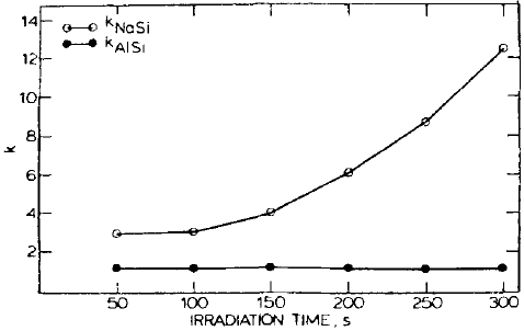
Figure 3776. Variations of kNaSi and kAlSi with irradiation time for albite feldspar (NaA1Si3O8) [1].
[1] McGill, R. J. and Hubbard, F. H. (1981) In Quantitative
Microanalysis with High Spatial Resolution (G. W.
Lorimer, M. N. Jacobs and P. Doig, eds.) The Metals
Society, London, 30.
|